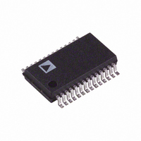
AD1854JRS Analog Devices Inc, AD1854JRS Datasheet - Page 6

AD1854JRS
Manufacturer Part Number
AD1854JRS
Description
IC DAC STEREO 96KHZ 5V 28SSOP
Manufacturer
Analog Devices Inc
Datasheet
1.AD1854JRSZ.pdf
(12 pages)
Specifications of AD1854JRS
Rohs Status
RoHS non-compliant
Number Of Bits
20
Data Interface
DSP, I²S, Serial
Number Of Converters
2
Voltage Supply Source
Analog and Digital
Power Dissipation (max)
250mW
Operating Temperature
0°C ~ 70°C
Mounting Type
Surface Mount
Package / Case
28-SSOP
For Use With
EVAL-AD1854EB - BOARD EVAL FOR AD1854
Settling Time
-
Available stocks
Company
Part Number
Manufacturer
Quantity
Price
Company:
Part Number:
AD1854JRS
Manufacturer:
MOTOROLA
Quantity:
1 157
Part Number:
AD1854JRS
Manufacturer:
ADI/亚德诺
Quantity:
20 000
Company:
Part Number:
AD1854JRSZ
Manufacturer:
ADI
Quantity:
26
Part Number:
AD1854JRSZ
Manufacturer:
ADI/亚德诺
Quantity:
20 000
AD1854
F
Normal, 32 kHz–48 kHz
Normal, 32 kHz–48 kHz
Normal, 32 kHz–48 kHz
Normal, 32 kHz–48 kHz
Double F
Double F
Double F
Double F
OPERATING FEATURES
Serial Data Input Port
The AD1854’s flexible serial data input port accepts data in
twos-complement, MSB-first format. The left channel data field
always precedes the right channel data field. The input data
consists of either 16, 18, 20, or 24 bits, as established by the
mode select pins (IDPM0 Pin 21 and IDPM1 Pin 20) or the
mode select bits (Bits 15 and 14) in the control register through
the SPI (Serial Peripheral Interface) control port. Neither the
pins nor the SPI controls has preference; to ensure proper control,
the selection not being used should be tied LO. Therefore,
when the SPI bits are used to control Serial Data Input Format,
Pins 20 and 21 should be tied LO. Similarly, when the pins are
to be used to select the Data Format, the SPI bits should be set
to zeros. When the SPI Control Port is not being used, the SPI
Pins (3, 4, and 5) should be tied LO.
Serial Data Input Mode
The AD1854 uses two multiplexed input pins to control the
mode configuration of the input data port mode as follows:
IDPM1
(Pin 20)
0
0
1
1
Bit Clock
S
L/RCLK
SDATA
L/RCLK
SDATA
INPUT
INPUT
INPUT
BCLK
INPUT
INPUT
INPUT
BCLK
S
S
S
S
(96 kHz)
(96 kHz)
(96 kHz)
(96 kHz)
LSB
IDPM0
(Pin 21)
0
1
0
1
0
Table I. Serial Data Input Modes
MSB
MSB–1
MSB–2
Serial Data Input Format
Right Justified (16 Bits)
I
Right Justified (20 Bits)
Right Justified (24 Bits)
Left Justified
2
S-Compatible
MSB
96/48
0
0
0
0
1
1
1
1
LEFT CHANNEL
MSB–1
LSB+2 LSB+1
LEFT CHANNEL
MSB–2
Table II. Frequency Mode Settings
Figure 1. Right-Justified Mode
LSB
Figure 2. I
MCLK
256 × F
384 × F
512 × F
128 × F
(384/2) × F
256 × F
LSB+2 LSB+1
2
S
S
S
S
S
S-Justified Mode
–6–
LSB
S
Figure 1 shows the right-justified mode (16-bit mode). L/RCLK
is HI for the left channel, LO for the right channel. Data is valid
on the rising edge of BCLK. The MSB is delayed 16-bit clock
periods from an L/RCLK transition, so that when there are 64
BCLK periods per L/RCLK period, the LSB of the data will be
right justified to the next L/RCLK transition. The right-justified
mode can also be used with 20-bit or 24-bit inputs as selected
in Table I.
Figure 2 shows the I
left channel and HI for the right channel. Data is valid on the
rising edge of BCLK. The MSB is left justified to an L/RCLK
transition but with a single BCLK period delay. The I
mode can be used with 16-/18-/20- or 24-bit inputs.
Figure 3 shows the left-justified mode. Note: Left-justified mode
is selected by pulsing IDPM1 (Pin 20) with bit clock, that is, tying
bit clock to IDPM1 while IDPM0 (Pin 21) is tied LO. Left-
justified can only be selected this way, it cannot be selected through
SPI Control Port.
L/RCLK is HI for the left channel, and LO for the right channel.
Data is valid on the rising edge of BCLK. The MSB is left-
justified to an L/RCLK transition, with no MSB delay. The
left-justified mode can be used with 16-/18-/20- or 24-bit inputs.
Note that the AD1854 is capable of a 32 × F
“packed mode” where the MSB is left-justified to an L/RCLK
transition, and the LSB is right-justified to an L/RCLK transi-
tion. L/RCLK is HI for the left channel, and LO for the right
channel. Data is valid on the rising edge of BCLK. Packed
mode can be used when the AD1854 is programmed in right-
justified mode. Packed mode is shown is Figure 4.
MSB
MSB–1
X2MCLK
0
0
1
1
0
0
1
1
MSB–2
RIGHT CHANNEL
MSB
2
S-justified mode. L/RCLK is LO for the
RIGHT CHANNEL
LSB+2 LSB+1
MSB–1
MSB–2
384/256
0
1
0
1
0
1
0
1
LSB
LSB+2 LSB+1
S
BCLK frequency
LSB
Note
Not Allowed
Not Allowed
2
MSB
S-justified
REV. A


