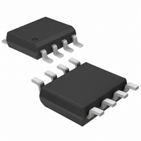
MAX5541CSA+T Maxim Integrated Products, MAX5541CSA+T Datasheet - Page 2

MAX5541CSA+T
Manufacturer Part Number
MAX5541CSA+T
Description
IC DAC 16BIT MONOTONIC SER 8SOIC
Manufacturer
Maxim Integrated Products
Datasheet
1.MAX5541ESA.pdf
(9 pages)
Specifications of MAX5541CSA+T
Settling Time
1µs
Number Of Bits
16
Data Interface
Serial
Number Of Converters
1
Voltage Supply Source
Single Supply
Power Dissipation (max)
1.5mW
Operating Temperature
0°C ~ 70°C
Mounting Type
Surface Mount
Package / Case
8-SOIC (3.9mm Width)
Lead Free Status / RoHS Status
Lead free / RoHS Compliant
ABSOLUTE MAXIMUM RATINGS
V
CS, SCLK, DIN to DGND..........................................-0.3V to +6V
REF to AGND, DGND ..................................-0.3V to (V
AGND to DGND.....................................................-0.3V to +0.3V
OUT to AGND, DGND.................................. ............-0.3V to V
Maximum Current into Any Pin............................................50mA
Continuous Power Dissipation (T
ELECTRICAL CHARACTERISTICS
(V
Low-Cost, +5V, Serial-Input,
Voltage-Output, 16-Bit DAC
Stresses beyond those listed under “Absolute Maximum Ratings” may cause permanent damage to the device. These are stress ratings only, and functional
operation of the device at these or any other conditions beyond those indicated in the operational sections of the specifications is not implied. Exposure to
absolute maximum rating conditions for extended periods may affect device reliability.
2
DYNAMIC PERFORMANCE—REFERENCE SECTION
DD
STATIC PERFORMANCE—ANALOG SECTION (R
REFERENCE INPUT
DYNAMIC PERFORMANCE—ANALOG SECTION (R
Resolution
Differential Nonlinearity
Integral Nonlinearity
Zero-Code Offset Error
Zero-Code Tempco
Gain Error (Note 2)
Gain-Error Tempco
DAC Output Resistance
Power-Supply Rejection
Reference Input Range
Reference Input Resistance
Voltage Output Slew-Rate
Output Settling Time
DAC Glitch Impulse
Digital Feedthrough
Reference -3dB Bandwidth
Reference Feedthrough
Signal-to-Noise Ratio
Reference Input Capacitance
DD
8-Pin SO (derate 5.88mW/°C above +70°C)................471mW
_______________________________________________________________________________________
to DGND............................................................-0.3V to +6V
= +5V ±5%, V
PARAMETER
REF
= +2.5V, V
A
AGND
= +70°C)
SYMBOL
ZS
R
V
R
DNL
PSR
SNR
ZSE
INL
BW
C
SR
OUT
REF
REF
N
= V
IN
TC
DGND
Guaranteed monotonic
V
T
T
T
T
T
(Note 3)
4.75V ≤ V
(Note 4)
(Note 5)
C
To ±
Major-carry transition
Code = 0000 hex, CS = V
SCLK = V
Code = FFFF hex
Code = 0000 hex, V
Code = 0000 hex
Code = FFFF hex
A
A
A
A
A
DD
L
= 0, T
= +25°C
= T
= T
= +25°C
= T
= 10pF (Note 6)
1
= 5V (Note 1)
/
L
2
DD
MIN
MIN
MIN
LSB of FS, C
= ∞)
A
L
+0.3V)
= T
= ∞)
DD
DIN
to T
to T
to T
MIN
≤ 5.25V
DD
= 0 to V
MAX
MAX
MAX
CONDITIONS
to T
L
REF
MAX
= 10pF
DD
Operating Temperature Ranges
Junction Temperature ......................................................+150°C
Storage Temperature Range .............................-65°C to +150°C
Lead Temperature (soldering, 10s) ................................ +300°C
= 1V
, unless otherwise noted. Typical values are at T
MAX5541CSA .....................................................0°C to +70°C
MAX5541ESA ..................................................-40°C to +85°C
levels
DD
,
P-P
at 100kHz
MIN
11.5
2.0
16
±0.05
±0.5
±0.1
TYP
6.25
120
±4
25
10
10
92
75
1
1
1
MAX
±1.0
±1.0
±16
±10
3.0
±1
±2
±5
A
= +25°C.)
ppm/°C
ppm/°C
UNITS
mV
MHz
V/µs
LSB
LSB
LSB
LSB
Bits
Bits
nVs
nVs
kΩ
kΩ
dB
µs
pF
V
P-P


