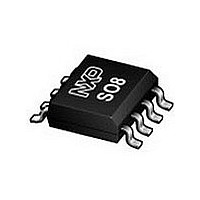
TJA1021T/20.118 NXP Semiconductors, TJA1021T/20.118 Datasheet - Page 14

TJA1021T/20.118
Manufacturer Part Number
TJA1021T/20.118
Description
Manufacturer
NXP Semiconductors
Datasheet
1.TJA1021T20.118.pdf
(25 pages)
Specifications of TJA1021T/20.118
Operating Supply Voltage (min)
5.5V
Operating Temperature Classification
Automotive
Mounting
Surface Mount
Pin Count
8
Lead Free Status / Rohs Status
Compliant
NXP Semiconductors
Table 8.
V
currents flow into the IC; typical values are given at V
[1]
[2]
[3]
[4]
TJA1021_5
Product data sheet
Symbol
Timing characteristics
t
t
t
t
t
t
t
t
t
t
t
t
f
r
PD(TX)
PD(TX)sym
PD(RX)
PD(RX)sym
wake(dom)LIN
wake(dom)WAKE_N
gotonorm
init(norm)
gotosleep
to(dom)TXD
BAT
3
4
t
(r-f)
All parameters are guaranteed by design over the virtual junction temperature range. Products are 100 % tested at 125 C ambient
temperature on wafer level (pre-testing). Cased products are 100 % tested at 25 C ambient temperature (final testing). Both pre-testing
and final testing use correlated test conditions to cover the specified temperature and power supply voltage range.
Not applicable for the /10 version of the TJA1021.
Bus load conditions are: C
= 5.5 V to 18 V; T
1
3
=
Dynamic characteristics
t
-------------------------------
bus rec min
2 t
Parameter
duty cycle 3
duty cycle 4
fall time
rise time
difference between rise
and fall time
transmitter propagation
delay
transmitter propagation
delay symmetry
receiver propagation
delay
receiver propagation
delay symmetry
dominant wake-up time
on pin LIN
dominant wake-up time
on pin WAKE_N
go to normal time
normal mode
initialization time
go to sleep time
TXD dominant time-out
time
bit
vj
= 40 C to +150 C; R
L
= 1 nF and R
…continued
L
= 1 k ; C
Conditions
V
V
t
V
V
t
V
V
t
V
V
t
V
Sleep mode
Sleep mode
time period for mode change from
Sleep, Power-on or Standby mode
into Normal mode
time period for mode change from
Normal slope mode into Sleep mode
V
bit
bit
bit
bit
th(rec)(max)
th(dom)(max)
th(rec)(max)
th(dom)(max)
th(rec)(min)
th(dom)(min)
th(rec)(min)
th(dom)(min)
BAT
TXD
L(LIN-VBAT)
= 96 s; V
= 96 s; V
= 96 s; V
= 96 s; V
Rev. 05 — 22 October 2009
= 7.3 V
L
= 0 V
= 6.8 nF and R
BAT
= 0.389
= 0.378
= 12 V; see
= 0.778
= 0.797
= 0.251
= 0.242
= 500 ; all voltages are defined with respect to ground; positive
= 0.616
= 0.630
BAT
BAT
BAT
BAT
= 7 V to 18 V
= 5.5 V to 7 V
= 7.6 V to 18 V
= 6.1 V to 7.6 V
L
V
V
V
V
= 660 ; C
V
V
V
V
BAT
BAT
Figure
BAT
BAT
BAT
BAT
BAT
BAT
;
;
;
;
;
;
;
;
5; unless otherwise specified.
L
= 10 nF and R
[3][4][7]
[3][4][7]
[4][5][7]
[4][5][7]
LIN 2.1/SAE J2602 transceiver
[2][4]
[2][4]
[2][4]
L
[2]
[6]
[6]
= 500 .
Min
0.417 -
0.417 -
-
-
-
-
-
-
30
7
2
5
2
27
5
2.5
2
Typ
-
-
-
-
-
-
-
-
-
80
30
5
-
5
55
© NXP B.V. 2009. All rights reserved.
TJA1021
[1]
Max
-
-
0.590
0.590
22.5
22.5
+5
6
+2.5
6
+2
150
50
10
20
10
90
14 of 25
Unit
ms
s
s
s
s
s
s
s
s
s
s
s
s


