AD664BD-BIP Analog Devices Inc, AD664BD-BIP Datasheet - Page 18
AD664BD-BIP
Manufacturer Part Number
AD664BD-BIP
Description
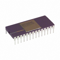
IC DAC 12BIT QUAD MONO 28-CDIP
Manufacturer
Analog Devices Inc
Datasheet
1.AD664JNZ-BIP.pdf
(20 pages)
Specifications of AD664BD-BIP
Data Interface
Parallel
Rohs Status
RoHS non-compliant
Settling Time
8µs
Number Of Bits
12
Number Of Converters
4
Voltage Supply Source
Dual ±
Power Dissipation (max)
525mW
Operating Temperature
-40°C ~ 85°C
Mounting Type
Through Hole
Package / Case
28-CDIP (0.600", 15.24mm)
Resolution (bits)
12bit
Sampling Rate
125kSPS
Supply Voltage Range - Digital
4.5V To 5.5V
Supply Current
15mA
Digital Ic Case Style
DIP
No. Of Pins
28
Number Of Channels
4
Resolution
12b
Conversion Rate
125KSPS
Interface Type
Parallel
Single Supply Voltage (typ)
Not RequiredV
Dual Supply Voltage (typ)
±15V
Architecture
R-2R
Power Supply Requirement
Dual
Output Type
Voltage
Integral Nonlinearity Error
±0.75LSB
Single Supply Voltage (min)
Not RequiredV
Single Supply Voltage (max)
Not RequiredV
Dual Supply Voltage (min)
±11.4V
Dual Supply Voltage (max)
±16.5V
Operating Temp Range
-40C to 85C
Operating Temperature Classification
Industrial
Mounting
Through Hole
Pin Count
28
Package Type
CDIP
Lead Free Status / Rohs Status
Not Compliant
Available stocks
Company
Part Number
Manufacturer
Quantity
Price

Company:
Part Number:
AD664BD-BIP
Manufacturer:
ADI
Quantity:
558
Part Number:
AD664BD-BIP
Manufacturer:
ADI/亚德诺
Quantity:
20 000


AD664
Simple AD664 to MC68000 Interface
Figure 28 shows an AD664 connected to an MC68000. In this
memory-mapped I/O scheme, the “left-justified” data is written
in one 12-bit input word. Four address bits are used to perform
the on-chip D/A selection as well as the various operating fea-
tures. The R/W signal controls the RD function and system
reset controls RST.
Figure 28. AD664 to MC68000 Interface
–18–
This scheme can be converted to write “right-justified’’ data by
connecting the data inputs to DATA bits D0 through D11
respectively. Other options include controlling the QS0, QS1
and QS2 pins with UDS and LDS to provide a way to write
8-bit input and read 8-bit output words.
REV. C
Related parts for AD664BD-BIP
Image
Part Number
Description
Manufacturer
Datasheet
Request
R

Part Number:
Description:
D/A Converter (D-A) IC
Manufacturer:
Analog Devices Inc
Datasheet:

Part Number:
Description:
±1.7g Dual-Axis IMEMS Accelerometer Evaluation Board
Manufacturer:
Analog Devices Inc
Datasheet:

Part Number:
Description:
Inertial Sensor Evaluation System
Manufacturer:
Analog Devices Inc
Datasheet:
Part Number:
Description:
Manufacturer:
Analog Devices Inc
Datasheet:
Part Number:
Description:
Manufacturer:
Analog Devices Inc
Datasheet:
Part Number:
Description:
Manufacturer:
Analog Devices Inc
Datasheet:
Part Number:
Description:
Manufacturer:
Analog Devices Inc
Datasheet:
Part Number:
Description:
Manufacturer:
Analog Devices Inc
Datasheet:
Part Number:
Description:
Manufacturer:
Analog Devices Inc
Datasheet:
Part Number:
Description:
Manufacturer:
Analog Devices Inc
Datasheet:
Part Number:
Description:
Manufacturer:
Analog Devices Inc
Datasheet:
Part Number:
Description:
Manufacturer:
Analog Devices Inc
Datasheet:
Part Number:
Description:
Manufacturer:
Analog Devices Inc
Datasheet: