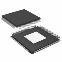
AD9779ABSVZ Analog Devices Inc, AD9779ABSVZ Datasheet - Page 38

AD9779ABSVZ
Manufacturer Part Number
AD9779ABSVZ
Description
IC DAC 16BIT 1.0GSPS 100TQFP
Manufacturer
Analog Devices Inc
Specifications of AD9779ABSVZ
Data Interface
Serial
Design Resources
Interfacing ADL5370 to AD9779A Dual-Channel, 1 GSPS High Speed DAC (CN0016) Interfacing ADL5371 to AD9779A Dual-Channel, 1 GSPS High Speed DAC (CN0017) Interfacing ADL5372 to AD9779A Dual-Channel, 1 GSPS High Speed DAC (CN0018) Interfacing ADL5373 to AD9779A Dual-Channel, 1 GSPS High Speed DAC (CN0019) Interfacing ADL5374 to AD9779A Dual-Channel, 1 GSPS High Speed DAC (CN0020) Interfacing ADL5375 to AD9779A Dual-Channel, 1 GSPS High Speed DAC (CN0021)
Number Of Bits
16
Number Of Converters
2
Voltage Supply Source
Analog and Digital
Power Dissipation (max)
300mW
Operating Temperature
-40°C ~ 85°C
Mounting Type
Surface Mount
Package / Case
100-TQFP Exposed Pad, 100-eTQFP, 100-HTQFP, 100-VQFP
Resolution (bits)
16bit
Sampling Rate
1GSPS
Input Channel Type
Parallel
Digital Ic Case Style
QFP
No. Of Pins
100
Operating Temperature Range
-40°C To +85°C
Number Of Channels
2
Resolution
16b
Interface Type
Parallel
Single Supply Voltage (typ)
3.3V
Dual Supply Voltage (typ)
Not RequiredV
Architecture
Interpolation Filter
Power Supply Requirement
Analog and Digital
Output Type
Current
Single Supply Voltage (min)
3.13V
Single Supply Voltage (max)
3.47V
Dual Supply Voltage (min)
Not RequiredV
Dual Supply Voltage (max)
Not RequiredV
Operating Temp Range
-40C to 85C
Operating Temperature Classification
Industrial
Mounting
Surface Mount
Pin Count
100
Package Type
TQFP EP
Lead Free Status / RoHS Status
Lead free / RoHS Compliant
For Use With
AD9779A-EBZ - BOARD EVALUATION FOR AD9779A
Settling Time
-
Lead Free Status / Rohs Status
Compliant
Available stocks
Company
Part Number
Manufacturer
Quantity
Price
Company:
Part Number:
AD9779ABSVZ
Manufacturer:
ADI
Quantity:
1
Company:
Part Number:
AD9779ABSVZ
Manufacturer:
ADI
Quantity:
184
Company:
Part Number:
AD9779ABSVZ
Manufacturer:
Analog Devices Inc
Quantity:
10 000
Part Number:
AD9779ABSVZ
Manufacturer:
ADI/亚德诺
Quantity:
20 000
Company:
Part Number:
AD9779ABSVZRL
Manufacturer:
Analog Devices Inc
Quantity:
10 000
AD9776A/AD9778A/AD9779A
If the optimal band is in the range of 32 to 62 (higher VCO
frequency), refer to Table 23.
Table 23. Setting Optimal PLL Band, When Band Is in the
Higher Range (32 to 62)
If System Startup
Temperature Is
−40°C to −30°C
−30°C to −10°C
−10°C to +15°C
15°C to 55°C
55°C to 85°C
Known Temperature Calibration with Memory
The preceding procedure requires temperature sensing upon
start-up or reset of the device to optimally choose the PLL band
select value that holds over the entire operating temperature
range. If temperature sensing is not available in the system, a
factory calibration at a known temperature is another method
for guaranteeing lock over temperature.
Factory calibration can be performed as follows:
1.
2.
3.
4.
5.
Set and Forget Device Option
If the PLL band select configuration methods described in
the previous sections cannot be implemented in a particular
system, there may be a screened device option that can satisfy
the system requirements. Analog Devices offers a pair of screened
devices that are guaranteed to maintain PLL lock over the entire
operating temperature range for a predetermined PLL band
select setting. This allows the user to preload a specific PLL
band select value for all devices that holds over temperature.
The values of N1 (Register 0x09, Bits<6:5>) and N2
(Register 0x09, Bits<4:3>) should be programmed along
with the PLL settings shown in Table 20.
Set the PLL band (Register 0x08, Bits<7:2>) to 63 to enable
PLL auto mode.
Wait for the PLL_LOCK pin or the PLL lock indicator
(Register 0x00, Bit 1) to go high. This should occur within
5 ms.
Read back the 6-bit PLL band (Register 0x08, Bits<7:2>).
Based on the temperature when the PLL auto band select is
performed, store into nonvolatile memory the PLL band
indicated in either Table 22 or Table 23. On system power-
up or restart, load the stored PLL band value into the PLL
band select parameter (Register 0x08, Bits<7:2>).
Set PLL Band as Follows
Set PLL band = readback band + 3
Set PLL band = readback band + 2
Set PLL band = readback band + 1
Set PLL band = readback band
Set PLL band = readback band − 1
Rev. A | Page 38 of 60
DRIVING THE REFCLK INPUT
The REFCLK input requires a low jitter differential drive signal.
The signal level can range from 400 mV p-p differential to
1.6 V p-p differential centered about a 400 mV input common-
mode voltage. Looking at the single-ended inputs, REFCLK+ or
REFCLK−, each input pin can safely swing from 200 mV p-p to
800 mV p-p about the 400 mV common-mode voltage. Although
these input levels are not directly LVDS compatible, REFCLK
can be driven by an offset ac-coupled LVDS signal, as shown in
Figure 72.
If a clean sine clock is available, it can be transformer-coupled
to REFCLK, as shown in Figure 72. Use of a CMOS or TTL
clock is also acceptable for lower sample rates. It can be routed
through a CMOS to LVDS translator, then ac-coupled, as
described in this section. Alternatively, it can be transformer-
coupled and clamped, as shown in Figure 73.
A simple bias network for generating V
It is important to use CVDD18 and CGND for the clock bias
circuit. Any noise or other signal that is coupled onto the clock
is multiplied by the DAC digital input signal and can degrade
DAC performance.
TTL OR CMOS
CLK INPUT
287Ω
1kΩ
LVDS_N_IN
LVDS_P_IN
Figure 73. TTL or CMOS REFCLK Drive Circuit
Figure 74. REFCLK V
Figure 72. LVDS REFCLK Drive Circuit
0.1µF
0.1µF
0.1µF
0.1µF
50Ω
50Ω
1nF
CM
Generator Circuit
V
V
CM
CM
1nF
CM
50Ω
50Ω
= 400mV
= 400mV
is shown in Figure 74.
REFCLK+
REFCLK–
BAV99ZXCT
HIGH SPEED
DUAL DIODE
V
CM
CVDD18
CGND
= 400mV
REFCLK+
REFCLK–


