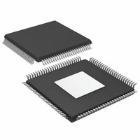
AD9779BSVZ Analog Devices Inc, AD9779BSVZ Datasheet - Page 41

AD9779BSVZ
Manufacturer Part Number
AD9779BSVZ
Description
IC DAC 16BIT DUAL 1GSPS 100TQFP
Manufacturer
Analog Devices Inc
Datasheet
1.AD9776BSVZRL.pdf
(56 pages)
Specifications of AD9779BSVZ
Data Interface
Serial
Number Of Bits
16
Number Of Converters
2
Voltage Supply Source
Analog and Digital
Power Dissipation (max)
300mW
Operating Temperature
-40°C ~ 85°C
Mounting Type
Surface Mount
Package / Case
100-TQFP Exposed Pad, 100-eTQFP, 100-HTQFP, 100-VQFP
Resolution (bits)
16bit
Sampling Rate
1GSPS
Input Channel Type
Parallel
Digital Ic Case Style
QFP
No. Of Pins
160
Operating Temperature Range
-40°C To +85°C
Lead Free Status / RoHS Status
Lead free / RoHS Compliant
For Use With
AD9779A-EBZ - BOARD EVALUATION FOR AD9779A
Settling Time
-
Lead Free Status / RoHS Status
Lead free / RoHS Compliant, Lead free / RoHS Compliant
Available stocks
Company
Part Number
Manufacturer
Quantity
Price
Company:
Part Number:
AD9779BSVZ
Manufacturer:
AD
Quantity:
2 100
Company:
Part Number:
AD9779BSVZ
Manufacturer:
ADI
Quantity:
325
Company:
Part Number:
AD9779BSVZ
Manufacturer:
Analog Devices Inc
Quantity:
10 000
Part Number:
AD9779BSVZ
Manufacturer:
ADI/亚德诺
Quantity:
20 000
Company:
Part Number:
AD9779BSVZRL
Manufacturer:
Analog Devices Inc
Quantity:
10 000
POWER-DOWN AND SLEEP MODES
The AD977x has a variety of power-down modes, so that the
digital engine, main TxDACs, or auxiliary DACs can be powered
down individually or together. Via the SPI port, the main TxDACs
can be placed in sleep or power-down mode. In sleep mode, the
TxDAC output is turned off, thus reducing power dissipation.
The reference remains powered on, however, so that recovery
from sleep mode is very fast. With the power-down mode bit
set (Register 0x00, Bit 4), all analog and digital circuitry, including
the reference, is powered down. The SPI port remains active in
this mode. This mode offers more substantial power savings
than sleep mode, but the turn-on time is much longer. The
auxiliary DACs also have the capability to be programmed into
sleep mode via the SPI port. The auto power-down enable bit
(Register 0x00, Bit 3) controls the power-down function for the
digital section of the devices. The auto power-down function
works in conjunction with the TXENABLE pin (Pin 39) according
to the following:
TXENABLE (Pin 39) =
or TXENABLE (Pin 39) =
As shown in Figure 90, the power dissipation saved by using the
power down mode is nearly proportional to the duty cycle of
the signal at the TXENABLE pin.
If the TxEnable invert bit (Register 0x02, Bit 1) is set, the
function of this TXENABLE pin is inverted.
0: autopower-down enable =
1: normal operation
0.9
0.8
0.7
0.6
0.5
0.4
0.3
0.2
0.1
Figure 90. Power Savings Based on Duty Cycle of TxEnable
0
0: flush data path with 0s
1: flush data for multiple REFCLK cycles; then
automatically place the digital engine in power-down
state. DACs, reference, and SPI port are not affected.
0
20
DUTY CYCLE (%)
40
60
2× INT
2× INT
4× INT
4× INT
8× INT
8× INT
f
f
f
f
f
f
DATA
DATA
DATA
DATA
DATA
DATA
80
= 50MSPS
= 200MSPS
= 50MSPS
= 200MSPS
= 50MSPS
= 200MSPS
100
Rev. A | Page 41 of 56
INTERLEAVED DATA MODE
The TxEnable bit is dual function. In dual port mode, it is
simply used to power down the digital section of the devices. In
interleaved mode, the IQ data stream is synchronized to
TXENABLE. Therefore, to achieve IQ synchronization,
TXENABLE should be held low until an I data word is present at
the inputs to Data Port 1. If a DATACLK rising edge occurs
while TXENABLE is at a high logic level, IQ data becomes
synchronized to the DATACLK output. TXENABLE can remain
high and the input IQ data remains synchronized. To be
backwards-compatible with previous DACs from Analog
Devices, Inc. such as the AD9777 and AD9786, the user can
also toggle TXENABLE once during each data input cycle, thus
continually updating the synchronization. If TXENABLE is
brought low and held low for multiple REFCLK cycles, then the
devices flush the data in the interpolation filters, and shut down
the digital engine after the filters are flushed. The amount of
REFCLK cycles it takes to go into this power-down mode is
then a function of the length of the equivalent 2×, 4×, or 8×
interpolation filter. The timing of TXENABLE, I/Q select, filter
flush, and digital power-down are shown in Figure 91.
The TXENABLE function can be inverted by changing the
status of Register 0x02, Bit 1. The other bit that controls IQ
ordering is the Q-first bit (Register 0x02, Bit 0). With the Q-first
bit reset to the default of 0, the IQ pairing that is latched is the
I1Q1, I2Q2, and so on. With IQ first set to 1, the first I data is
discarded and the pairing is I2Q1, I3Q2, and so on. Note that
with IQ-first set, the I data is still routed to the internal I
channel, the Q data is routed to the internal Q channel, and
only the pairing changes.
TIMING INFORMATION
Figure 92 to Figure 95 show some of the various timing
possibilities when the PLL is enabled. The combination of the
settings of N2 and N3 from Figure 74 means that the reference
clock frequency can be a multiple of the actual input data rate.
Figure 92 to Figure 95 show, respectively, what the timing looks
like when N2/N3 = 1 and 2.
In interleaved mode, set-up and hold times of DATACLK out to
data in are the same as those shown in Figure 92 to Figure 95. It
is recommended that any toggling of TXENABLE occur
concurrently with the digital data input updating. In this way,
timing margins between DATACLK, TXENABLE, and digital
input data are optimized.
INTERLEAVED
INPUT DATA
TxENABLE
TxENABLE CAN REMAIN
I/Q SYNCHRONIZATION
HIGH OR TOGGLE FOR
Figure 91. TXENABLE Function
I1
AD9776/AD9778/AD9779
Q1
INTERPOLATION
FLUSHING
FILTERS
I2
Q2
DOWN DIGITAL
SECTION
POWER


