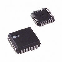
AD7846JP Analog Devices Inc, AD7846JP Datasheet - Page 8

AD7846JP
Manufacturer Part Number
AD7846JP
Description
IC DAC 16BIT LC2MOS VOUT 28PLCC
Manufacturer
Analog Devices Inc
Datasheet
1.AD7846JPZ.pdf
(24 pages)
Specifications of AD7846JP
Data Interface
Parallel
Rohs Status
RoHS non-compliant
Settling Time
7µs
Number Of Bits
16
Number Of Converters
1
Voltage Supply Source
Dual ±
Power Dissipation (max)
100mW
Operating Temperature
0°C ~ 70°C
Mounting Type
Surface Mount
Package / Case
28-LCC (J-Lead)
Resolution (bits)
16bit
Sampling Rate
143kSPS
Input Channel Type
Parallel
Supply Voltage Range - Digital
4.75V To 5.25V
Supply Current
5mA
Digital Ic Case Style
LCC
Lead Free Status / RoHS Status
Contains lead / RoHS non-compliant
Available stocks
Company
Part Number
Manufacturer
Quantity
Price
Company:
Part Number:
AD7846JP
Manufacturer:
AD
Quantity:
1 980
Company:
Part Number:
AD7846JP
Manufacturer:
AD
Quantity:
5 510
Part Number:
AD7846JP
Manufacturer:
ADI/亚德诺
Quantity:
20 000
Company:
Part Number:
AD7846JP-REEL
Manufacturer:
AD
Quantity:
5 510
Company:
Part Number:
AD7846JP-REEL
Manufacturer:
LT
Quantity:
5 510
Company:
Part Number:
AD7846JP-REEL
Manufacturer:
Analog Devices Inc
Quantity:
10 000
Company:
Part Number:
AD7846JPZ
Manufacturer:
Analog Devices Inc
Quantity:
10 000
Part Number:
AD7846JPZ
Manufacturer:
ADI/亚德诺
Quantity:
20 000
Company:
Part Number:
AD7846JPZ-REEL
Manufacturer:
Analog Devices Inc
Quantity:
10 000
AD7846
TYPICAL PERFORMANCE CHARACTERISTICS
30
25
20
15
10
8
7
6
5
4
3
2
1
0
Figure 9. AC Feedthrough, V
5
0
100
10
V
V
V
V
V
V
V
V
GAIN = +2
DD
SS
REF +
REF –
Figure 10. AC Feedthrough to V
DD
SS
REF+
REF–
1V
A1
Figure 11. Large Signal Frequency Response
= –15V
= +15V
= +15V
= –15V
100
= +1V rms
= 0V
= ±5V SINE WAVE
= 0V
–0.40V
2mV
1k
1k
FREQUENCY (Hz)
FREQUENCY (Hz)
REF+
10k
10k
20µs
= 1 V rms, 10 kHz Sine Wave
OUT
100k
vs. Frequency
100k
1M
10M
1M
Rev. G | Page 8 of 24
Figure 13. Digital-to-Analog Glitch Impulse Without Internal Deglitcher
Figure 14. Digital-to-Analog Glitch Impulse with Internal Deglitcher
500
450
400
350
300
250
200
150
100
50
0
100
DATA
LDAC
DATA
V
V
V
GAIN = +1
DAC LOADED WITH ALL 1s
OUT
OUT
REF+
(10…000 to 011…111 Transition)
(10…000 to 011…111 Transition)
= V
Figure 12. Noise Spectral Density
REF–
1k
= 0V
FREQUENCY (Hz)
0.5µs/DIV
1µs/DIV
10k
50mV/DIV
50mV/DIV
5V/DIV
5V/DIV
100k
5V/DIV
1M


