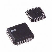
AD7846JP Analog Devices Inc, AD7846JP Datasheet - Page 3

AD7846JP
Manufacturer Part Number
AD7846JP
Description
IC DAC 16BIT LC2MOS VOUT 28PLCC
Manufacturer
Analog Devices Inc
Datasheet
1.AD7846JPZ.pdf
(24 pages)
Specifications of AD7846JP
Data Interface
Parallel
Rohs Status
RoHS non-compliant
Settling Time
7µs
Number Of Bits
16
Number Of Converters
1
Voltage Supply Source
Dual ±
Power Dissipation (max)
100mW
Operating Temperature
0°C ~ 70°C
Mounting Type
Surface Mount
Package / Case
28-LCC (J-Lead)
Resolution (bits)
16bit
Sampling Rate
143kSPS
Input Channel Type
Parallel
Supply Voltage Range - Digital
4.75V To 5.25V
Supply Current
5mA
Digital Ic Case Style
LCC
Lead Free Status / RoHS Status
Contains lead / RoHS non-compliant
Available stocks
Company
Part Number
Manufacturer
Quantity
Price
Company:
Part Number:
AD7846JP
Manufacturer:
AD
Quantity:
1 980
Company:
Part Number:
AD7846JP
Manufacturer:
AD
Quantity:
5 510
Part Number:
AD7846JP
Manufacturer:
ADI/亚德诺
Quantity:
20 000
Company:
Part Number:
AD7846JP-REEL
Manufacturer:
AD
Quantity:
5 510
Company:
Part Number:
AD7846JP-REEL
Manufacturer:
LT
Quantity:
5 510
Company:
Part Number:
AD7846JP-REEL
Manufacturer:
Analog Devices Inc
Quantity:
10 000
Company:
Part Number:
AD7846JPZ
Manufacturer:
Analog Devices Inc
Quantity:
10 000
Part Number:
AD7846JPZ
Manufacturer:
ADI/亚德诺
Quantity:
20 000
Company:
Part Number:
AD7846JPZ-REEL
Manufacturer:
Analog Devices Inc
Quantity:
10 000
SPECIFICATIONS
V
R
Table 1.
Parameter
RESOLUTION
UNIPOLAR OUTPUT
BIPOLAR OUTPUT
REFERENCE INPUT
OUTPUT CHARACTERISTICS
DIGITAL INPUTS
IN
DD
Relative Accuracy at +25°C
Differential Nonlinearity Error
Gain Error at +25°C
Offset Error at +25°C
Gain TC
Offset TC
Relative Accuracy at +25°C
Differential Nonlinearity Error
Gain Error at +25°C
Offset Error at +25°C
Bipolar Zero Error at +25°C
Gain TC
Offset TC
Bipolar Zero TC
Input Resistance
V
V
Output Voltage Swing
Resistive Load
Capacitive Load
Output Resistance
Short Circuit Current
V
V
I
C
IN
connected to 0 V. All specifications T
REF+
REF−
IH
IL
IN
= +14.25 V to +15.75 V; V
T
T
T
T
T
T
T
(Input Current)
(Input Low Voltage)
(Input High Voltage)
(Input Capacitance)
MIN
MIN
MIN
MIN
MIN
MIN
MIN
Range
Range
to T
to T
to T
to T
to T
to T
to T
2
2
1
2
2
MAX
MAX
MAX
MAX
MAX
MAX
MAX
2
2
SS
= −14.25 V to –15.75 V; V
MIN
J, A Versions
16
±12
±16
±1
±12
±16
±12
±16
±1
±1
±6
±8
±1
±6
±16
±6
±16
±6
±12
±1
±1
±1
20
40
V
V
V
V
V
V
2
1000
0.3
±25
2.4
0.8
±10
10
SS
DD
SS
DD
SS
DD
to T
+ 6 to
+ 6 to
+ 4 to
− 6
− 6
− 3
MAX
, unless otherwise noted.
CC
16
±4
±8
±0.5
±6
±16
±6
±16
±2
±4
±0.5
±4
±16
±4
±12
±4
±8
40
V
V
V
0.3
±25
±10
10
K, B Versions
±1
±1
±1
±1
±1
20
V
V
V
2
1000
2.4
0.8
Rev. G | Page 3 of 24
SS
DD
SS
DD
SS
DD
= +4.75 V to +5.25 V. V
+ 6 to
+ 6 to
+ 4 to
− 6
− 6
− 3
Unit
Bits
LSB typ
LSB max
LSB max
LSB typ
LSB max
LSB typ
LSB max
ppm FSR/°C typ
ppm FSR/°C typ
LSB typ
LSB max
LSB max
LSB typ
LSB max
LSB typ
LSB max
LSB typ
LSB max
ppm FSR/°Ctyp
ppm FSR/°Ctyp
ppm FSR/°Ctyp
kΩ min
kΩ max
V min to
V max
V min to
V max
V max
kΩ min
pF max
Ω typ
mA typ
V min
V max
μA max
pF max
OUT
loaded with 2 kΩ, 1000 pF to 0 V; V
Test Conditions/Comments
V
1 LSB = 153 μV
All grades guaranteed monotonic
V
V
1 LSB = 305 μV
All grades guaranteed monotonic
V
V
Resistance from V
Typically 30 kΩ
To 0 V
To 0 V
To 0 V or any power supply
REF−
OUT
REF−
OUT
OUT
load = 10 MΩ
load = 10 MΩ
load = 10 MΩ
= 0 V, V
= –5 V, V
OUT
OUT
= 0 V to +10 V
= −10 V to +10 V
REF+
to V
REF−
REF+
AD7846
= +5 V;


