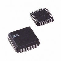
AD7846JP Analog Devices Inc, AD7846JP Datasheet - Page 6

AD7846JP
Manufacturer Part Number
AD7846JP
Description
IC DAC 16BIT LC2MOS VOUT 28PLCC
Manufacturer
Analog Devices Inc
Datasheet
1.AD7846JPZ.pdf
(24 pages)
Specifications of AD7846JP
Data Interface
Parallel
Rohs Status
RoHS non-compliant
Settling Time
7µs
Number Of Bits
16
Number Of Converters
1
Voltage Supply Source
Dual ±
Power Dissipation (max)
100mW
Operating Temperature
0°C ~ 70°C
Mounting Type
Surface Mount
Package / Case
28-LCC (J-Lead)
Resolution (bits)
16bit
Sampling Rate
143kSPS
Input Channel Type
Parallel
Supply Voltage Range - Digital
4.75V To 5.25V
Supply Current
5mA
Digital Ic Case Style
LCC
Lead Free Status / RoHS Status
Contains lead / RoHS non-compliant
Available stocks
Company
Part Number
Manufacturer
Quantity
Price
Company:
Part Number:
AD7846JP
Manufacturer:
AD
Quantity:
1 980
Company:
Part Number:
AD7846JP
Manufacturer:
AD
Quantity:
5 510
Part Number:
AD7846JP
Manufacturer:
ADI/亚德诺
Quantity:
20 000
Company:
Part Number:
AD7846JP-REEL
Manufacturer:
AD
Quantity:
5 510
Company:
Part Number:
AD7846JP-REEL
Manufacturer:
LT
Quantity:
5 510
Company:
Part Number:
AD7846JP-REEL
Manufacturer:
Analog Devices Inc
Quantity:
10 000
Company:
Part Number:
AD7846JPZ
Manufacturer:
Analog Devices Inc
Quantity:
10 000
Part Number:
AD7846JPZ
Manufacturer:
ADI/亚德诺
Quantity:
20 000
Company:
Part Number:
AD7846JPZ-REEL
Manufacturer:
Analog Devices Inc
Quantity:
10 000
AD7846
ABSOLUTE MAXIMUM RATINGS
Table 4.
Parameter
V
V
V
V
V
V
R
Digital Input Voltage to DGND
Digital Output Voltage to DGND
Power Dissipation (Any Package)
Operating Temperature Range
Storage Temperature Range
Lead Temperature (Soldering)
1
V
dissipation of the package is not exceeded.
IN
DD
CC
SS
REF+
REF−
OUT
OUT
To +75°C
Derates above +75°C
J, K Versions
A, B Versions
to DGND
to DGND
to DGND
to DGND
to DGND
can be shorted to DGND, V
to DGND
to DGND
1
DD
, V
SS
, or V
Rating
−0.4 V to +17 V
−0.4 V, V
(whichever is lower)
+0.4 V to −17 V
V
V
V
(whichever is lower)
V
−0.4 V to V
−0.4 V to V
1000 mW
10 mW/°C
0°C to +70°C
−40°C to +85°C
−65°C to +150°C
+300°C
CC
DD
DD
DD
DD
provided that the power
+ 0.4 V, V
+ 0.4 V, V
+ 0.4 V, V
+ 0.4 V, V
DD
CC
CC
+ 0.4 V, or +7 V
SS
SS
SS
SS
+ 0.4 V
+ 0.4 V
− 0.4 V, or ±10 V
− 0.4 V
− 0.4 V
− 0.4 V
Rev. G | Page 6 of 24
Stresses above those listed under Absolute Maximum Ratings
may cause permanent damage to the device. This is a stress
rating only; functional operation of the device at these or any
other conditions above those indicated in the operational
section of this specification is not implied. Exposure to absolute
maximum rating conditions for extended periods may affect
device reliability.
ESD CAUTION


