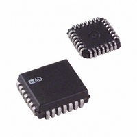
DAC8413FPC Analog Devices Inc, DAC8413FPC Datasheet - Page 17

DAC8413FPC
Manufacturer Part Number
DAC8413FPC
Description
IC DAC 12BIT QUAD READBK 28-PLCC
Manufacturer
Analog Devices Inc
Datasheet
1.DAC8412FPCZ.pdf
(20 pages)
Specifications of DAC8413FPC
Rohs Status
RoHS non-compliant
Settling Time
6µs
Number Of Bits
12
Data Interface
Parallel
Number Of Converters
4
Voltage Supply Source
Single Supply
Power Dissipation (max)
330mW
Operating Temperature
-40°C ~ 85°C
Mounting Type
Surface Mount
Package / Case
28-LCC (J-Lead)
Number Of Channels
4
Resolution
12b
Conversion Rate
167KSPS
Interface Type
Parallel
Single Supply Voltage (typ)
5V
Dual Supply Voltage (typ)
±15V
Architecture
R-2R
Power Supply Requirement
Single/Dual
Output Type
Voltage
Integral Nonlinearity Error
±4LSB
Single Supply Voltage (min)
4.75V
Single Supply Voltage (max)
5.25V
Dual Supply Voltage (min)
±14.25V
Dual Supply Voltage (max)
±15.75V
Operating Temp Range
-40C to 85C
Operating Temperature Classification
Industrial
Mounting
Surface Mount
Pin Count
28
Package Type
PLCC
Lead Free Status / Rohs Status
Not Compliant
Available stocks
Company
Part Number
Manufacturer
Quantity
Price
Company:
Part Number:
DAC8413FPC
Manufacturer:
VISHAY
Quantity:
6 652
Company:
Part Number:
DAC8413FPC
Manufacturer:
Analog Devices Inc
Quantity:
10 000
Part Number:
DAC8413FPC
Manufacturer:
ADI/亚德诺
Quantity:
20 000
Company:
Part Number:
DAC8413FPC-REEL
Manufacturer:
Analog Devices Inc
Quantity:
10 000
Company:
Part Number:
DAC8413FPCZ
Manufacturer:
Analog Devices Inc
Quantity:
10 000
Company:
Part Number:
DAC8413FPCZ-REEL
Manufacturer:
Analog Devices Inc
Quantity:
10 000
The 0.2 μF bypass capacitors shown at the reference inputs in
Figure 40 should be used whenever ±10 V references are used.
Applications with single references or references to ±5 V may
not require the 0.2 μF bypassing. The 6.2 Ω resistor in series
with the output of the reference amplifier keeps the amplifier
from oscillating with the capacitive load. This 6.2 Ω resistor has
been found to be large enough to stabilize this circuit. Larger
resistor values are acceptable, provided that the drop across the
resistor does not exceed V
and a maximum current of 2.75 mA, then the resistor should be
under 200 Ω for the loading of a single DAC8412.
Using two separate references is not recommended. Having two
references can cause different drifts with time and temperature;
whereas with a single reference, most drifts track.
Unipolar positive full-scale operation can usually be set with a
reference with the correct output voltage. This is preferable to
using a reference and dividing down to the required value. For a
10 V full-scale output, the circuit can be configured as shown in
Figure 41. In this configuration, the full-scale value is set first by
adjusting the 10 kΩ resistor for a full-scale output of 9.9976 V.
GND
REF08
10kΩ
–15V
TRIM
10µF
0.01µF
OUTPUT
0.2µF
Figure 41. Unipolar –10 V Operation
ZERO TO –10V OPERATION
BE
. Assuming a minimum V
V
V
REFH
REFL
DAC8412
DAC8413
V
OR
V
DD
SS
BE
0.1µF
//10µF
of 0.6 V
Rev. F | Page 17 of 20
Figure 41 shows the DAC8412 configured for –10 V to 0 V
operation. A REF08 with a –10 V output is connected directly
to V
SINGLE +5 V SUPPLY OPERATION
For operation with a 5 V supply, the reference voltage should be
set between 1.0 V and 2.5 V for optimum linearity. Figure 42
shows a REF43 used to supply a 2.5 V reference voltage. The
headroom of the reference and DAC are both sufficient to support
a 5 V supply with ±5% tolerance. V
connected to the same supply. Separate bypassing to each pin
should also be used.
REFL
REF43
5V
for the reference voltage.
GND
INPUT
OUTPUT
TRIM
10µF
ZERO TO 2.5V OPERATION
Figure 42. +5 V Single-Supply Operation
SINGLE 5V SUPPLY
10kΩ
0.01µF
0.2µF
V
V
REFH
REFL
DAC8412/DAC8413
DD
and V
DAC8412
DAC8413
OR
V
V
DD
SS
LOGIC
should be
0.1µF
//10µF


