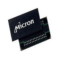
MT47H32M8BP-3:B Micron Technology Inc, MT47H32M8BP-3:B Datasheet - Page 101

MT47H32M8BP-3:B
Manufacturer Part Number
MT47H32M8BP-3:B
Description
Manufacturer
Micron Technology Inc
Type
DDR2 SDRAMr
Datasheet
1.MT47H32M8BP-3B.pdf
(128 pages)
Specifications of MT47H32M8BP-3:B
Organization
32Mx8
Density
256Mb
Address Bus
15b
Access Time (max)
450ps
Maximum Clock Rate
667MHz
Operating Supply Voltage (typ)
1.8V
Package Type
FBGA
Operating Temp Range
0C to 85C
Operating Supply Voltage (max)
1.9V
Operating Supply Voltage (min)
1.7V
Supply Current
190mA
Pin Count
60
Mounting
Surface Mount
Operating Temperature Classification
Commercial
Lead Free Status / Rohs Status
Compliant
Available stocks
Company
Part Number
Manufacturer
Quantity
Price
Company:
Part Number:
MT47H32M8BP-3:B
Manufacturer:
MICRON
Quantity:
586
Company:
Part Number:
MT47H32M8BP-3:B TR
Manufacturer:
Micron Technology Inc
Quantity:
10 000
Figure 57: Consecutive WRITE-to-WRITE
Figure 58: Nonconsecutive WRITE-to-WRITE
PDF: 09005aef8117c187
256MbDDR2.pdf - Rev. M 7/09 EN
Notes:
Notes:
t DQSS (NOM)
t DQSS (NOM)
DQS, DQS#
DQS, DQS#
Command
Command
1. Subsequent rising DQS signals must align to the clock within
2. DI b, etc. = data-in for column b, etc.
3. Three subsequent elements of data-in are applied in the programmed order following
4. Three subsequent elements of data-in are applied in the programmed order following
5. Shown with BL = 4, AL = 0, CL = 3; thus, WL = 2.
6. Each WRITE command may be to any bank.
1. Subsequent rising DQS signals must align to the clock within
2. DI b (or n), etc. = data-in for column b (or column n).
3. Three subsequent elements of data-in are applied in the programmed order following
4. Three subsequent elements of data-in are applied in the programmed order following
5. Shown with BL = 4, AL = 0, CL = 3; thus, WL = 2.
6. Each WRITE command may be to any bank.
Address
Address
DI b.
DI n.
DI b.
DI n.
CK#
CK#
DM
DM
DQ
DQ
CK
CK
WRITE
WRITE
Bank,
Bank,
Col b
Col b
T0
T0
WL ±
WL = 2
t CCD
WL = 2
NOP
NOP
T1
T1
t
DQSS
WL ± t DQSS
T1n
101
WRITE
NOP
Bank,
Col n
T2
DI
b
T2
DI
b
T2n
T2n
Micron Technology, Inc. reserves the right to change products or specifications without notice.
WRITE
WL = 2
Bank,
Col n
T3
1
NOP
1
T3
256Mb: x4, x8, x16 DDR2 SDRAM
T3n
T3n
WL = 2
NOP
T4
NOP
T4
1
DI
n
Transitioning Data
Transitioning Data
T4n
T4n
1
NOP
T5
DI
n
NOP
1
T5
©2003 Micron Technology, Inc. All rights reserved.
t
t
DQSS.
DQSS.
T5n
T5n
NOP
1
T6
NOP
Don’t Care
T6
Don’t Care
T6n
WRITE


