AD7840ARS Analog Devices Inc, AD7840ARS Datasheet - Page 7
AD7840ARS
Manufacturer Part Number
AD7840ARS
Description
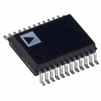
IC DAC 14BIT LOW POWER 5V 24SSOP
Manufacturer
Analog Devices Inc
Datasheet
1.AD7840ARSZ.pdf
(16 pages)
Specifications of AD7840ARS
Rohs Status
RoHS non-compliant
Settling Time
2.5µs
Number Of Bits
14
Data Interface
Serial, Parallel
Number Of Converters
1
Voltage Supply Source
Dual ±
Power Dissipation (max)
100mW
Operating Temperature
-25°C ~ 85°C
Mounting Type
Surface Mount
Package / Case
24-SSOP
Available stocks
Company
Part Number
Manufacturer
Quantity
Price

Part Number:
AD7840ARSZ
Manufacturer:
ADI/亚德诺
Quantity:
20 000


REV. B
CS
H
X
L
H
H
X
f
L
g
X = Don’t Care
Figure 7. AD7840 Simplified Parallel Input Control Logic
WR
X
H
L
H
X
H
f
g
L
Figure 6. Parallel Mode Timing Diagram
Table III. Parallel Mode Truth Table
LDAC
H
H
H
L
L
L
L
L
Function
}
Input Latch Transparent
}
Input Latch Transparent
DAC Latch Data Transfer Inhibited
}
Both Latches Latched
Input Latch Is Latched
DAC Latch Data Transfer Occurs
DAC Latch Transparent
Analog Output Updated
Input Latch Latched
–7–
Serial Data Format
The serial data format is selected for the AD7840 by connecting
the CS/SERIAL line to –5 V. In this case, the WR/SYNC,
D13/SDATA, D12/SCLK, D11/FORMAT and D10/JUSTIFY
pins all assume their serial functions. The unused parallel inputs
should not be left unconnected to avoid noise pickup. Serial
data is loaded to the input latch under control of SCLK, SYNC
and SDATA. The AD7840 expects a 16-bit stream of serial data
on its SDATA input. Serial data must be valid on the falling
edge of SCLK. The SYNC input provides the frame synchroni-
zation signal which tells the AD7840 that valid serial data will
be available for the next 16 falling edges of SCLK. Figure 8
shows the timing diagram for serial data format.
Although 16 bits of data are clocked into the AD7840, only 14
bits go into the input latch. Therefore, two bits in the stream are
don’t cares since their value does not affect the input latch data.
The order and position in which the AD7840 accepts the 14 bits
of input data depends upon the FORMAT and JUSTIFY in-
puts. There are four different input data modes which can be
chosen (see Table I in the Pin Function Description section).
The first mode (M1) assumes that the first two bits of the input
data stream are don’t cares, the third bit is the LSB and the last
(or 16th bit) is the MSB. This mode is chosen by tying both the
FORMAT and JUSTIFY pins to a logic 0. The second mode
(M2; FORMAT = 0, JUSTIFY = 1) assumes that the first bit in
the data stream is the LSB, the fourteenth bit is the MSB and
the last two bits are don’t cares. The third mode (M3;
FORMAT= 1, JUSTIFY 0) assumes that the first two bits in
the stream are again don’t cares, the third bit is now the MSB
and the sixteenth bit is the LSB. The final mode (M4; FOR-
MAT = 1, JUSTIFY= 1) assumes that the first bit is the MSB,
the fourteenth bit is the LSB and the last two bits of the stream
are don’t cares.
Figure 8. Serial Mode Timing Diagram
AD7840
Related parts for AD7840ARS
Image
Part Number
Description
Manufacturer
Datasheet
Request
R

Part Number:
Description:
±1.7g Dual-Axis IMEMS Accelerometer Evaluation Board
Manufacturer:
Analog Devices Inc
Datasheet:

Part Number:
Description:
Inertial Sensor Evaluation System
Manufacturer:
Analog Devices Inc
Datasheet:
Part Number:
Description:
Manufacturer:
Analog Devices Inc
Datasheet:
Part Number:
Description:
Manufacturer:
Analog Devices Inc
Datasheet:
Part Number:
Description:
Manufacturer:
Analog Devices Inc
Datasheet:
Part Number:
Description:
Manufacturer:
Analog Devices Inc
Datasheet:
Part Number:
Description:
Manufacturer:
Analog Devices Inc
Datasheet:
Part Number:
Description:
Manufacturer:
Analog Devices Inc
Datasheet:
Part Number:
Description:
Manufacturer:
Analog Devices Inc
Datasheet:
Part Number:
Description:
Manufacturer:
Analog Devices Inc
Datasheet:
Part Number:
Description:
Manufacturer:
Analog Devices Inc
Datasheet:
Part Number:
Description:
Manufacturer:
Analog Devices Inc
Datasheet:
Part Number:
Description:
Manufacturer:
Analog Devices Inc
Datasheet: