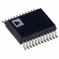
AD7840ARS Analog Devices Inc, AD7840ARS Datasheet - Page 11

AD7840ARS
Manufacturer Part Number
AD7840ARS
Description
IC DAC 14BIT LOW POWER 5V 24SSOP
Manufacturer
Analog Devices Inc
Datasheet
1.AD7840ARSZ.pdf
(16 pages)
Specifications of AD7840ARS
Rohs Status
RoHS non-compliant
Settling Time
2.5µs
Number Of Bits
14
Data Interface
Serial, Parallel
Number Of Converters
1
Voltage Supply Source
Dual ±
Power Dissipation (max)
100mW
Operating Temperature
-25°C ~ 85°C
Mounting Type
Surface Mount
Package / Case
24-SSOP
Available stocks
Company
Part Number
Manufacturer
Quantity
Price
Part Number:
AD7840ARSZ
Manufacturer:
ADI/亚德诺
Quantity:
20 000
REV. B
AD7840–68000 Interface
An interface between the AD7840 and the 68000 microproces-
sor is shown in Figure 19. In this interface example, the LDAC
input is hardwired low. As a result the DAC latch and analog
output are updated on the rising edge of WR. A single move
instruction, therefore, loads the input latch and updates the output.
MOVE.W D0,$DAC
D0 = 68000 D0 Register
DAC = AD7840 Address
Serial Interfacing
Figures 20 to 23 show the AD7840 configured for serial inter-
facing with the CS input hardwired to –5 V. The parallel bus is
not activated during serial communication with the AD7840.
AD7840–ADSP-2101/ADSP-2102 Serial Interface
Figure 20 shows a serial interface between the AD7840 and the
ADSP-2101/ADSP-2102 DSP processor. Also included in the
interface is the AD7870, a 12-bit A/D converter. An interface
such as this is suitable for modem and other applications which
have a DAC and an ADC in serial communication with a
microprocessor.
The interface uses just one of the two serial ports of the
ADSP-2101/ADSP-2102. Conversion is initiated on the
AD7870 at a fixed sample rate (e.g., 9.6 kHz) which is provided
by a timer or clock recovery circuitry. While communication
takes place between the ADC and the ADSP-2101/ ADSP-2102,
the AD7870 SSTRB line is low. This SSTRB line is used to
provide a frame synchronization pulse for the AD7840 SYNC
and ADSP-2101/ADSP-2102 TFS lines. This means that com-
munication between the processor and the AD7840 can only
take place while the AD7870 is communicating with the processor.
This arrangement is desirable in systems such as modems where
the DAC and ADC communication should be synchronous.
The use of the AD7870 SCLK for the AD7840 SCLK and
ADSP-2101/ADSP-2102 SCLK means that only one serial port
of the processor is used. The serial clock for the AD7870 must
be set for continuous clock for correct operation of this interface.
Data from the ADSP-2101/ADSP-2102 is valid on the falling
edge of SCLK. The LDAC input of the AD7840 is permanently
Figure 19. AD7840–MC68000 Parallel Interface
–11–
low so the update of the DAC latch and analog output takes
place on the sixteenth falling edge of SCLK (with SYNC low).
The FORMAT pin of the AD7840 must be tied to +5 V and
the JUSTIFY pin tied to DGND for this interface to operate
correctly.
AD7840–DSP56000 Serial Interface
A serial interface between the AD7840 and the DSP56000 is
shown in Figure 21. The DSP56000 is configured for normal
mode synchronous operation with gated clock. It is also set up
for a 16-bit word with SCK and SC2 as outputs and the FSL
control bit set to a 0. SCK is internally generated on the
DSP56000 and applied to the AD7840 SCLK input. Data from
the DSP56000 is valid on the falling edge of SCK. The SC2
output provides the framing pulse for valid data. This line must
be inverted before being applied to the SYNC input of the
AD7840.
The LDAC input of the AD7840 is connected to DGND so the
update of the DAC latch takes place on the sixteenth falling
edge of SCLK. As with the previous interface, the FORMAT
pin of the AD7840 must be tied to +5 V and the JUSTIFY pin
tied to DGND.
Figure 20. Complete DAC/ADC Serial Interface
Figure 21. AD7840–DSP56000 Serial Interface
AD7840


