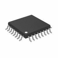
AD5763CSUZ-REEL7 Analog Devices Inc, AD5763CSUZ-REEL7 Datasheet - Page 18

AD5763CSUZ-REEL7
Manufacturer Part Number
AD5763CSUZ-REEL7
Description
DAC 16BIT DUAL 5V 2LSB 32-TQFP
Manufacturer
Analog Devices Inc
Datasheet
1.AD5763CSUZ.pdf
(28 pages)
Specifications of AD5763CSUZ-REEL7
Design Resources
High Accuracy, Bipolar Voltage Output Digital-to-Analog Conversion Using AD5763 (CN0074)
Settling Time
8µs
Number Of Bits
16
Data Interface
Serial
Number Of Converters
2
Voltage Supply Source
Dual ±
Power Dissipation (max)
45mW
Operating Temperature
-40°C ~ 105°C
Mounting Type
Surface Mount
Package / Case
32-TQFP, 32-VQFP
Lead Free Status / RoHS Status
Lead free / RoHS Compliant
Available stocks
Company
Part Number
Manufacturer
Quantity
Price
Company:
Part Number:
AD5763CSUZ-REEL7
Manufacturer:
Analog Devices Inc
Quantity:
10 000
AD5763
TRANSFER FUNCTION
Table 7 shows the ideal input code to output voltage relationship
for the AD5763 for both offset binary and twos complement
data coding.
Table 7. Ideal Output Voltage to Input Code Relationship
Digital Input
Offset Binary Data Coding
MSB
1111
1000
1000
0111
0000
Twos Complement Data Coding
MSB
0111
0000
0000
1111
1000
Table 8. Input Register Format
MSB
DB23
R/W
Table 9. Input Register Bit Functions
Bit
R/W
REG2, REG1, REG0
A2, A1, A0
D15:D0
1111
0000
0000
1111
0000
1111
0000
0000
1111
0000
DB22
0
1111
0000
0000
1111
0000
1111
0000
0000
1111
0000
DB21
REG2
Description
Indicates a read from or a write to the addressed register
These bits are used in association with the address bits to determine if a read or write operation is sent to the
function register, data register, offset register, or gain register
REG2
0
0
0
1
1
These bits are used to decode the DAC channels
A2
0
0
1
Data bits
1111
0001
0000
1111
0000
1111
0001
0000
1111
0000
DB20
REG1
LSB
LSB
Analog Output
VOUTx
+2V
+2V
0 V
−2V
−2V
VOUTx
+2V
+2V
0 V
−2V
−2V
REG1
0
1
1
0
0
A1
0
0
0
DB19
REG0
REF
REF
REF
REF
REF
REF
REF
REF
× (32,767/32,768)
× (1/32,768)
× (1/32,768)
× (32,767/32,768)
× (32,767/32,768)
× (1/32,768)
× (1/32,768)
× (32,767/32,768)
REG0
0
0
1
0
1
A0
0
1
0
DB18
A2
DB17
A1
Function
Function register
Data register
Coarse gain register
Fine gain register
Offset register
Channel Address
DAC A
DAC B
Both DACs
Rev. A | Page 18 of 28
DB16
A0
The output voltage expression for the AD5763 is given by
where:
D is the decimal equivalent of the code loaded to the DAC.
V
ASYNCHRONOUS CLEAR (CLR)
CLR is a negative edge triggered clear that allows the outputs to
be cleared to either 0 V (twos complement coding) or negative
full scale (offset binary coding). It is necessary to keep CLR low
for a minimum amount of time for the operation to complete (see
Figure 2). When the CLR signal is returned high, the output
remains at the cleared value until a new value is programmed.
If at power-on, CLR is at 0 V, all DAC outputs are updated with
the clear value. A clear can also be initiated through software by
writing a command, 0x04XXXX, to the AD5763.
REFIN
VOUTx
is the reference voltage applied at the REFA and REFB pins.
2
V
REFIN
4
DB15:DB0
V
Data
REFIN
65
D
,
536
LSB


