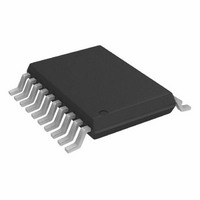
AD7305BRUZ Analog Devices Inc, AD7305BRUZ Datasheet - Page 9

AD7305BRUZ
Manufacturer Part Number
AD7305BRUZ
Description
IC DAC 8BIT QUAD R-R 20-TSSOP
Manufacturer
Analog Devices Inc
Datasheet
1.AD7304BRZ-REEL.pdf
(20 pages)
Specifications of AD7305BRUZ
Data Interface
Parallel
Settling Time
1µs
Number Of Bits
8
Number Of Converters
4
Voltage Supply Source
Dual ±
Power Dissipation (max)
60mW
Operating Temperature
-40°C ~ 85°C
Mounting Type
Surface Mount
Package / Case
20-TSSOP
Resolution (bits)
8bit
Sampling Rate
1MSPS
Input Channel Type
Parallel
Supply Voltage Range - Analog
2.7V To 5.5V
Supply Current
6mA
Digital Ic Case Style
TSSOP
Number Of Channels
4
Resolution
8b
Interface Type
Parallel
Single Supply Voltage (typ)
3/5V
Dual Supply Voltage (typ)
±5V
Architecture
R-2R
Power Supply Requirement
Single/Dual
Output Type
Voltage
Single Supply Voltage (min)
2.7V
Single Supply Voltage (max)
5.5V
Dual Supply Voltage (min)
±4.5V
Dual Supply Voltage (max)
±5.5V
Operating Temp Range
-40C to 85C
Operating Temperature Classification
Industrial
Mounting
Surface Mount
Pin Count
20
Package
20TSSOP
Conversion Rate
1 MSPS
Digital Interface Type
Parallel
Number Of Outputs Per Chip
4
Full Scale Error
±4 LSB
Integral Nonlinearity Error
±1 LSB
Maximum Settling Time
2 us
Lead Free Status / RoHS Status
Lead free / RoHS Compliant
Lead Free Status / RoHS Status
Lead free / RoHS Compliant, Lead free / RoHS Compliant
Available stocks
Company
Part Number
Manufacturer
Quantity
Price
Part Number:
AD7305BRUZ
Manufacturer:
ADI/亚德诺
Quantity:
20 000
Table 8. AD7305 Pin Function Description
Pin No.
1
2
3
4
5
6
7
8
9
10
11
12
13
14
15
16
17
18
19
20
Mnemonic
V
V
V
V
GND
LDAC
DB7
DB6
DB5
DB4
DB3
DB2
DB1
DB0
WR
A1
A0/SHDN
V
V
V
OUT
OUT
SS
REF
DD
OUT
OUT
B
A
D
C
Description
Channel B Rail-to-Rail Buffered DAC Voltage Output. Full-scale set by reference voltage applied to V
open circuit when SHDN is enabled.
Channel A Rail-to-Rail Buffered DAC Voltage Output. Full-scale set by reference voltage applied to V
open circuit when SHDN is enabled.
Negative Power Supply Input. Specified range of operation is 0 V to –5.5 V.
Channel B Reference Input. Establishes V
Common Analog and Digital Ground.
Load DAC Register Strobe, Active Low. Simultaneously transfers data from all four input registers into the
corresponding DAC registers. Asynchronous active low input. DAC register is transparent when LDAC = 0. See Table 6
for operation.
MSB Digital Input Data Bit.
Data Bit 6.
Data Bit 5.
Data Bit 4.
Data Bit 3.
Data Bit 2.
Data Bit 1.
LSB Digital Input Data Bit.
Write Data into Input Register Control Line, Active Low. See Table 6 for operation.
Address Bit 1.
Address Bit 0/Hardware Shutdown (SHDN) Control Input, Active When Pin Is Left Floating by a Three-State Logic
Driver. Does not effect DAC register contents as long as power is present on V
Positive Power Supply Input. Specified range of operation is 2.7 V to 5.5 V.
Channel D Rail-to-Rail Buffered DAC Voltage Output. Full-scale set by reference voltage applied to V
open circuit when SHDN is enabled.
Channel C Rail-to-Rail Buffered DAC Voltage Output. Full-scale set by reference voltage applied to V
open circuit when SHDN is enabled.
V
V
LDAC
OUT
OUT
V
GND
DB7
DB6
DB5
DB4
Figure 9. AD7305 Pin Configuration
V
REF
SS
B
A
10
1
2
3
4
5
6
7
8
9
Rev. C | Page 9 of 20
(Not to Scale)
AD7305
TOP VIEW
OUT
full-scale voltage. Specified range of operation is V
20
19
18
17
16
15
14
13
12
11
V
V
V
A0/SHDN
A1
WR
DB0
DB1
DB2
DB3
OUT
OUT
DD
C
D
DD
.
AD7304/AD7305
SS
< V
REF
REF
REF
REF
REF
B pin. Output is
A pin. Output is
C pin. Output is
D pin. Output is
< V
DD
.


