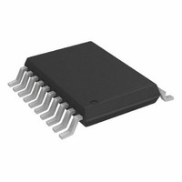
AD7305BRUZ Analog Devices Inc, AD7305BRUZ Datasheet - Page 16

AD7305BRUZ
Manufacturer Part Number
AD7305BRUZ
Description
IC DAC 8BIT QUAD R-R 20-TSSOP
Manufacturer
Analog Devices Inc
Datasheet
1.AD7304BRZ-REEL.pdf
(20 pages)
Specifications of AD7305BRUZ
Data Interface
Parallel
Settling Time
1µs
Number Of Bits
8
Number Of Converters
4
Voltage Supply Source
Dual ±
Power Dissipation (max)
60mW
Operating Temperature
-40°C ~ 85°C
Mounting Type
Surface Mount
Package / Case
20-TSSOP
Resolution (bits)
8bit
Sampling Rate
1MSPS
Input Channel Type
Parallel
Supply Voltage Range - Analog
2.7V To 5.5V
Supply Current
6mA
Digital Ic Case Style
TSSOP
Number Of Channels
4
Resolution
8b
Interface Type
Parallel
Single Supply Voltage (typ)
3/5V
Dual Supply Voltage (typ)
±5V
Architecture
R-2R
Power Supply Requirement
Single/Dual
Output Type
Voltage
Single Supply Voltage (min)
2.7V
Single Supply Voltage (max)
5.5V
Dual Supply Voltage (min)
±4.5V
Dual Supply Voltage (max)
±5.5V
Operating Temp Range
-40C to 85C
Operating Temperature Classification
Industrial
Mounting
Surface Mount
Pin Count
20
Package
20TSSOP
Conversion Rate
1 MSPS
Digital Interface Type
Parallel
Number Of Outputs Per Chip
4
Full Scale Error
±4 LSB
Integral Nonlinearity Error
±1 LSB
Maximum Settling Time
2 us
Lead Free Status / RoHS Status
Lead free / RoHS Compliant
Lead Free Status / RoHS Status
Lead free / RoHS Compliant, Lead free / RoHS Compliant
Available stocks
Company
Part Number
Manufacturer
Quantity
Price
Part Number:
AD7305BRUZ
Manufacturer:
ADI/亚德诺
Quantity:
20 000
AD7304/AD7305
AD7305 PARALLEL DATA INTERFACE
The AD7305 has an 8-bit parallel interface DB7 = MSB, DB0 =
LSB. Two address bits, A1 and A0, are decoded when an active
low write strobe is placed on the WR pin, see Table 6. The WR
is a level-sensitive input pin, therefore, the data setup and data
hold times defined in the Timing Specifications section need to
be adhered to.
DB0–DB7
The LDAC pin provides the capability of simultaneously
updating all DAC registers with new data from the input
registers at the same time. This results in the analog outputs all
changing to their new values at the same time. The LDAC pin is
a level-sensitive input. If the simultaneous update feature is not
required, the LDAC pin can be tied to logic low. When the
A0/SHDN
DATA
WR
A1
640k
80kΩ
280k
Figure 36. AD7305 Equivalent Logic Interface
2:4
DECODE
8
Ω
Ω
DAC A
GND
V
320k
680k
DD
B
C
D
Ω
Ω
POWER-
RESET
REGISTER
REGISTER
REGISTER
REGISTER
ON
INPUT
INPUT
INPUT
INPUT
AD7305
R
R
R
R
LDAC
REGISTER
REGISTER
REGISTER
REGISTER
DAC B
DAC C
DAC D
DAC A
V
REF
R
R
R
R
V
DD
DAC B
DAC A
DAC C
DAC D
OE
OE
OE
OE
V
SS
V
V
V
V
OUT
OUT
OUT
OUT
Rev. C | Page 16 of 20
A
B
C
D
LDAC is tied to Logic Low, the DAC registers become
transparent and the input register data determines the DAC
output voltage (see Figure 36 for an equivalent interface logic
diagram).
AD7226 PIN COMPATIBILITY
By tying the LDAC pin to ground, the AD7305 has the same pin
configuration and functionality as the AD7226, with the
exception of a lower power supply operating voltage.
AD7305 HARDWARE SHUTDOWN SHDN
If a three-state driver is used on the A0/SHDN pin, the AD7305
can be placed into a power shutdown mode when the A0/SHDN
pin is placed in a high impedance state. For proper operation,
no other termination voltages should be present on this pin. An
internal window comparator detects when the logic voltage on
the SHDN pin is between 28% and 36% of V
ance, internal-bias generator provides this voltage on the SHDN
pin. The four DAC output voltages become high impedance
with a nominal resistance of 120 kΩ to ground.
ESD PROTECTION CIRCUITS
All logic input pins contain back-biased ESD protection Zeners
connected to ground (GND). The V
biased ESD protection Zener connected to V
DIGITAL
INPUTS
Figure 37. Equivalent ESD Protection Circuits
GND
V
V
REF
DD
REF
X
pins also contain a back-
DD
DD
. A high imped-
(see Figure 37).


