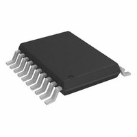
AD7305BRUZ Analog Devices Inc, AD7305BRUZ Datasheet - Page 14

AD7305BRUZ
Manufacturer Part Number
AD7305BRUZ
Description
IC DAC 8BIT QUAD R-R 20-TSSOP
Manufacturer
Analog Devices Inc
Datasheet
1.AD7304BRZ-REEL.pdf
(20 pages)
Specifications of AD7305BRUZ
Data Interface
Parallel
Settling Time
1µs
Number Of Bits
8
Number Of Converters
4
Voltage Supply Source
Dual ±
Power Dissipation (max)
60mW
Operating Temperature
-40°C ~ 85°C
Mounting Type
Surface Mount
Package / Case
20-TSSOP
Resolution (bits)
8bit
Sampling Rate
1MSPS
Input Channel Type
Parallel
Supply Voltage Range - Analog
2.7V To 5.5V
Supply Current
6mA
Digital Ic Case Style
TSSOP
Number Of Channels
4
Resolution
8b
Interface Type
Parallel
Single Supply Voltage (typ)
3/5V
Dual Supply Voltage (typ)
±5V
Architecture
R-2R
Power Supply Requirement
Single/Dual
Output Type
Voltage
Single Supply Voltage (min)
2.7V
Single Supply Voltage (max)
5.5V
Dual Supply Voltage (min)
±4.5V
Dual Supply Voltage (max)
±5.5V
Operating Temp Range
-40C to 85C
Operating Temperature Classification
Industrial
Mounting
Surface Mount
Pin Count
20
Package
20TSSOP
Conversion Rate
1 MSPS
Digital Interface Type
Parallel
Number Of Outputs Per Chip
4
Full Scale Error
±4 LSB
Integral Nonlinearity Error
±1 LSB
Maximum Settling Time
2 us
Lead Free Status / RoHS Status
Lead free / RoHS Compliant
Lead Free Status / RoHS Status
Lead free / RoHS Compliant, Lead free / RoHS Compliant
Available stocks
Company
Part Number
Manufacturer
Quantity
Price
Part Number:
AD7305BRUZ
Manufacturer:
ADI/亚德诺
Quantity:
20 000
AD7304/AD7305
CIRCUIT OPERATION
The AD7304/AD7305 are 4-channel, 8-bit, voltage output
DACs, differing primarily in digital logic interface and number
of reference inputs. Both parts share the same internal DAC
design and true rail-to-rail output buffers. The AD7304 contains
four independent multiplying reference inputs, while the
AD7305 has one common reference input. The AD7304 uses a
3-wire SPI-compatible serial data interface, while the AD7305
offers an 8-bit parallel data interface.
DAC SECTION
Each part contains four voltage-switched R-2R ladder DACs.
Figure 33 shows a typical equivalent DAC. These DACs are
designed to operate both single-supply or dual-supply,
depending on whether the user supplies a negative voltage on
the V
ground. In either mode, the DAC output voltage is determined
by the V
the corresponding DAC register according to Equation 1.
Note that the output full-scale polarity is the same as the V
polarity for dc reference voltages.
V
SS
OUT
pin. In a single-supply application, the V
REF
= V
input voltage and the digital data (D) loaded into
REF
V
Figure 33. Typical Equivalent DAC Channel
REF
D/256
DB7
DB6
DB0
2R
2R
2R
R
2R
V
V
DD
SS
V
OUT
SS
is tied to
REF
Rev. C | Page 14 of 20
(1)
These DACs are also designed to accommodate ac reference
input signals. As long as the ac signals are maintained between
V
multiplying bandwidth performance. In order to use negative
input reference voltages, the V
negative voltage of equal or greater magnitude than the
reference voltage.
The reference inputs are code dependent, exhibiting worst-case
minimum resistance values specified in the parametric specifi-
cation table. The DAC outputs V
are each capable of driving 2 kΩ loads in parallel with up to 500 pF
loads. Output sink current and source current are shown in
Figure 10 and Figure 11, respectively. The output slew rate is
nominally 3.6 V/µs while operating from ±5 V supplies. The
low output impedance of the buffers minimizes crosstalk
between analog input channels. At 100 kHz, 65 dB of channel-
to-channel isolation exists (Figure 26). Output voltage noise is
plotted in Figure 23. In order to maintain good analog perform-
ance, power supply bypassing of 0.01 µF in parallel with 1 µF is
recommended. The true rail-to-rail capability of the AD7304/AD7305
allows the user to connect the reference inputs directly to the
same supply as the V
conditions, clean power supply voltages (low ripple, avoid
switching supplies) appropriate for the application should be
used.
SS
< V
REF
< V
Figure 34. Equivalent DAC Amplifier Output Circuit
DD
, the user can expect 50 kHz of full power,
DD
or V
Q1
Q2
SS
pin (Figure 34). Under these
SS
V
V
DD
SS
pin must be biased with a
OUT
120kΩ
A, V
OUT
V
OUT
B, V
X
OUT
C, and V
OUT
D


