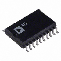
DAC312HS Analog Devices Inc, DAC312HS Datasheet - Page 4

DAC312HS
Manufacturer Part Number
DAC312HS
Description
IC DAC 12BIT MULTIPLY HS 20-SOIC
Manufacturer
Analog Devices Inc
Datasheet
1.DAC312HPZ.pdf
(14 pages)
Specifications of DAC312HS
Mounting Type
Surface Mount
Package / Case
20-SOIC (7.5mm Width)
Rohs Status
RoHS non-compliant
Settling Time
250ns
Number Of Bits
12
Data Interface
Parallel
Number Of Converters
1
Voltage Supply Source
Dual ±
Power Dissipation (max)
375mW
Operating Temperature
-40°C ~ 85°C
Resolution (bits)
12bit
No. Of Pins
20
Peak Reflow Compatible (260 C)
No
No. Of Bits
12 Bit
Leaded Process Compatible
No
Interface Type
Serial
Lead Free Status / RoHS Status
Contains lead / RoHS non-compliant
Available stocks
Company
Part Number
Manufacturer
Quantity
Price
Part Number:
DAC312HS-REEL
Manufacturer:
ADI/亚德诺
Quantity:
20 000
Company:
Part Number:
DAC312HSREEL
Manufacturer:
TOSHIBA
Quantity:
4 082
Part Number:
DAC312HSZ
Manufacturer:
ADI/亚德诺
Quantity:
20 000
Part Number:
DAC312HSZ-REEL
Manufacturer:
ADI/亚德诺
Quantity:
20 000
DAC312
DICE CHARACTERISTICS
WAFER TEST LIMITS
Parameter
Resolution
Monotonicity
Nonlinearity
Output Voltage
Full-Scale
Full-Scale Symmetry
Zero-Scale Current
Differential
Logic Input Levels “0”
Logic Input Levels “1”
Logic Input Swing
Reference Bias
Power Supply
Power Supply
Power
NOTE
Electrical tests are performed at wafer probe to the limits shown. Due to variations in assembly methods and normal yield loss, yield after packaging is not guaranteed
for standard product dice. Consult factory to negotiate specifications based on dice lot qualification through sample lot assembly and testing.
DIE SIZE 0.141
Compliance
Current
Nonlinearity
Current
Sensitivity
Current
Dissipation
0.096 inch, 13,536 sq. mils (3.58
Symbol
Voc
I
I
DNL
V
V
V
I
PSSI
PSSI
I+
I–
P
FSS
ZS
15
D
IL
IH
IS
@ V
FS+
FS–
S
=
15 V, I
Ideal Step Size
Conditions
Full-Scale Current
Change <1/2 LSB
V
R
Deviation from
V
V
V+ = +13.5 V to +16.5 V, V– = –15 V
V– = –13.5 V to –16.5 V, V+ = +15 V
V
I
V
I
REF
REF
REF
14
LC
LC
S
S
REF
= +15 V
= +15 V
, R
= GND
= GND
= 1.0 mA, T
= 10.000 V
15
1.0 mA
1.0 mA
= 10.000 k
2.44 mm, 8.74 sq. mm)
A
= 25 C, unless otherwise noted. Output characteristics refer to both I
–4–
10. B10
1. B1 (MSB)
2. B2
3. B3
4. B4
5. B5
6. B6
7. B7
8. B8
9. B9
DAC312N
Limit
12
12
+10
–5
4.031
3.967
0.1
0.8
2
+18
–5
–2
7
–18
375
0.05
1
0.012
1/2
0.001
0.001
DAC312G
Limit
12
12
+10
–5
4.063
3.935
0.1
0.8
2
+18
–5
–2
7
–18
375
0.05
2
0.025
1
0.001
0.001
11. B11
12. B12 (LSB)
13. V
14. V
15. V
16. COMP
17. V–
18. I
19. I
20. V+
O
O
LC
REF
REF
/A
(+)
(–)
GND
Units
Bits min
Bits min
%FS max
V max
mA min
%FS max
V min
mW max
V min
mA max
Bits (LSB) max
V max
V max
V min
%/%max
mA max
A max
A max
A max
REV. C
OUT
and I
OUT
.


