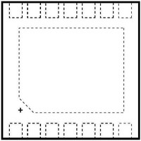
DS4402N+ Maxim Integrated Products, DS4402N+ Datasheet

DS4402N+
Specifications of DS4402N+
Related parts for DS4402N+
DS4402N+ Summary of contents
Page 1
... C-Compatible Serial Interface ♦ Two Three-Level Address Pins Allow Nine Applications Devices on Same I ♦ Small Package (14-Pin TDFN) ♦ -40°C to +85°C Temperature Range ♦ 2.7V to 5.5V Operation PART DS4402N+ 14 OUT3 (N.C.) DS4402N+T& DS4404N+ CC DS4404N+T&R OUT2 (N.C Denotes a lead(Pb)-free/RoHS-compliant package T& ...
Page 2
Two/Four-Channel, I ABSOLUTE MAXIMUM RATINGS Voltage Range SDA, and SCL CC Relative to Ground.............................................-0.5V to +6.0V Voltage Range on A0, A1, FS0, FS1, FS2, FS3, OUT0, OUT1, OUT2, and OUT3 Relative to Ground ................-0. ...
Page 3
Two/Four-Channel, I OUTPUT CURRENT CHARACTERISTICS (continued +2.7V to +5.5V -40°C to +85°C.) CC PARAMETER Output-Current Power-Supply Rejection Ratio Output Leakage Current at Zero Current Setting Output-Current Differential Linearity Output-Current Integral Linearity ...
Page 4
Two/Four-Channel, I PIN NAME DS4404 DS4402 1 1 SDA 2 2 SCL 3 3 GND 4 — FS3 5 — FS2 6 6 FS1 7 7 FS0 8 8 OUT0 10 10 OUT1 12 — OUT2 14 — OUT3 9, ...
Page 5
Two/Four-Channel, I Detailed Description The DS4402/DS4404 contain two/four I current sources (Figure 1) that are each capable of sinking and sourcing current. Each output has 31 sink and 31 source settings that are programmed through 2 the I C interface. ...
Page 6
Two/Four-Channel, I Memory Organization To control the DS4402/DS4404’s current sources, write to the memory addresses listed in Table 2. Table 2. Memory Addresses MEMORY ADDRESS CURRENT SOURCE (HEXADECIMAL) F8h F9h FAh* FBh* *Only for DS4404. The format of each output ...
Page 7
Two/Four-Channel, I Acknowledgement (ACK and NACK): An Acknowledge- ment (ACK) or Not Acknowledge (NACK) is always the ninth bit transmitted during a byte transfer. The device receiving data (the master during a read or the slave during a write operation) ...
Page 8
Two/Four-Channel, I Applications Information Example Calculations for an Adjustable Power Supply Using the typical circuit, assuming a typical output volt- age of 2.0V, a feedback voltage of 0.8V 500Ω, and R2 = 333Ω, to adjust or margin the ...
Page 9
... Maxim cannot assume responsibility for use of any circuitry other than circuitry entirely embodied in a Maxim product. No circuit patent licenses are implied. Maxim reserves the right to change the circuitry and specifications without notice at any time. Maxim Integrated Products, 120 San Gabriel Drive, Sunnyvale, CA 94086 408-737-7600 _____________________ 9 © 2009 Maxim Integrated Products is a registered trademark of Dallas Semiconductor Corporation ...


