AD5601BKSZ-500RL7 Analog Devices Inc, AD5601BKSZ-500RL7 Datasheet - Page 6
AD5601BKSZ-500RL7
Manufacturer Part Number
AD5601BKSZ-500RL7
Description
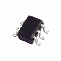
IC DAC 8BIT BUFF V-OUT SC70-6
Manufacturer
Analog Devices Inc
Series
nanoDAC™r
Datasheet
1.AD5601BKSZ-REEL7.pdf
(20 pages)
Specifications of AD5601BKSZ-500RL7
Data Interface
Serial
Settling Time
6µs
Number Of Bits
8
Number Of Converters
1
Voltage Supply Source
Single Supply
Power Dissipation (max)
500µW
Operating Temperature
-40°C ~ 125°C
Mounting Type
Surface Mount
Package / Case
SC-70-6, SC-88, SOT-363
Resolution (bits)
8bit
Sampling Rate
1.7MSPS
Input Channel Type
Serial
Supply Voltage Range - Analog
2.7V To 5.5V
Supply Current
75µA
Digital Ic Case Style
SC-70
Number Of Channels
1
Resolution
8b
Conversion Rate
1.7MSPS
Interface Type
SER 3W SPI QSPI UW
Single Supply Voltage (typ)
3.3/5V
Dual Supply Voltage (typ)
Not RequiredV
Architecture
Resistor-String
Power Supply Requirement
Single
Output Type
Voltage
Integral Nonlinearity Error
±0.5+/- LSB
Single Supply Voltage (min)
2.7V
Single Supply Voltage (max)
5.5V
Dual Supply Voltage (min)
Not RequiredV
Dual Supply Voltage (max)
Not RequiredV
Operating Temp Range
-40C to 125C
Operating Temperature Classification
Automotive
Mounting
Surface Mount
Pin Count
6
Package Type
SC-70
Lead Free Status / RoHS Status
Lead free / RoHS Compliant
Lead Free Status / RoHS Status
Lead free / RoHS Compliant, Lead free / RoHS Compliant
Available stocks
Company
Part Number
Manufacturer
Quantity
Price

Part Number:
AD5601BKSZ-500RL7
Manufacturer:
ADI/亚德诺
Quantity:
20 000


AD5601/AD5611/AD5621
PIN CONFIGURATION AND FUNCTION DESCRIPTIONS
Table 5. Pin Function Descriptions
Pin No.
1
2
3
4
5
6
Mnemonic
SYNC
SCLK
SDIN
V
GND
V
DD
OUT
Description
Level-Triggered Control Input (Active Low). This is the frame synchronization signal for the input data. When SYNC
goes low, it enables the input shift register, and data is transferred in on the falling edges of the clocks that follow.
The DAC is updated following the 16
rising edge of SYNC acts as an interrupt and the write sequence is ignored by the DAC.
Serial Clock Input. Data is clocked into the input shift register on the falling edge of the serial clock input. Data can
be transferred at rates up to 30 MHz.
Serial Data Input. This device has a 16-bit shift register. Data is clocked into the register on the falling edge of the
serial clock input.
Power Supply Input. The AD5601/AD5611/AD5621 can be operated from 2.7 V to 5.5 V. V
Ground. Ground reference point for all circuitry on the AD5601/AD5611/AD5621.
Analog Output Voltage from the DAC. The output amplifier has rail-to-rail operation.
Figure 3. 6-Lead SC70 Pin Configuration
SYNC
SCLK
SDIN
1
2
3
Rev. E | Page 6 of 20
th
(Not to Scale)
clock cycle, unless SYNC is taken high before this edge, in which case the
AD5601/
AD5611/
AD5621
TOP VIEW
6
5
4
V
GND
V
OUT
DD
DD
should be decoupled to GND.
Related parts for AD5601BKSZ-500RL7
Image
Part Number
Description
Manufacturer
Datasheet
Request
R

Part Number:
Description:
IC,D/A CONVERTER,SINGLE,8-BIT,CMOS,TSSOP,6PIN
Manufacturer:
Analog Devices Inc
Datasheet:

Part Number:
Description:
±1.7g Dual-Axis IMEMS Accelerometer Evaluation Board
Manufacturer:
Analog Devices Inc
Datasheet:

Part Number:
Description:
Inertial Sensor Evaluation System
Manufacturer:
Analog Devices Inc
Datasheet:
Part Number:
Description:
Manufacturer:
Analog Devices Inc
Datasheet:
Part Number:
Description:
Manufacturer:
Analog Devices Inc
Datasheet:
Part Number:
Description:
Manufacturer:
Analog Devices Inc
Datasheet:
Part Number:
Description:
Manufacturer:
Analog Devices Inc
Datasheet:
Part Number:
Description:
Manufacturer:
Analog Devices Inc
Datasheet:
Part Number:
Description:
Manufacturer:
Analog Devices Inc
Datasheet:
Part Number:
Description:
Manufacturer:
Analog Devices Inc
Datasheet:
Part Number:
Description:
Manufacturer:
Analog Devices Inc
Datasheet:
Part Number:
Description:
Manufacturer:
Analog Devices Inc
Datasheet:
Part Number:
Description:
Manufacturer:
Analog Devices Inc
Datasheet: