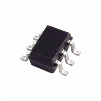
AD5601BKSZ-500RL7 Analog Devices Inc, AD5601BKSZ-500RL7 Datasheet - Page 19

AD5601BKSZ-500RL7
Manufacturer Part Number
AD5601BKSZ-500RL7
Description
IC DAC 8BIT BUFF V-OUT SC70-6
Manufacturer
Analog Devices Inc
Series
nanoDAC™r
Datasheet
1.AD5601BKSZ-REEL7.pdf
(20 pages)
Specifications of AD5601BKSZ-500RL7
Data Interface
Serial
Settling Time
6µs
Number Of Bits
8
Number Of Converters
1
Voltage Supply Source
Single Supply
Power Dissipation (max)
500µW
Operating Temperature
-40°C ~ 125°C
Mounting Type
Surface Mount
Package / Case
SC-70-6, SC-88, SOT-363
Resolution (bits)
8bit
Sampling Rate
1.7MSPS
Input Channel Type
Serial
Supply Voltage Range - Analog
2.7V To 5.5V
Supply Current
75µA
Digital Ic Case Style
SC-70
Number Of Channels
1
Resolution
8b
Conversion Rate
1.7MSPS
Interface Type
SER 3W SPI QSPI UW
Single Supply Voltage (typ)
3.3/5V
Dual Supply Voltage (typ)
Not RequiredV
Architecture
Resistor-String
Power Supply Requirement
Single
Output Type
Voltage
Integral Nonlinearity Error
±0.5+/- LSB
Single Supply Voltage (min)
2.7V
Single Supply Voltage (max)
5.5V
Dual Supply Voltage (min)
Not RequiredV
Dual Supply Voltage (max)
Not RequiredV
Operating Temp Range
-40C to 125C
Operating Temperature Classification
Automotive
Mounting
Surface Mount
Pin Count
6
Package Type
SC-70
Lead Free Status / RoHS Status
Lead free / RoHS Compliant
Lead Free Status / RoHS Status
Lead free / RoHS Compliant, Lead free / RoHS Compliant
Available stocks
Company
Part Number
Manufacturer
Quantity
Price
Part Number:
AD5601BKSZ-500RL7
Manufacturer:
ADI/亚德诺
Quantity:
20 000
USING THE AD5601/AD5611/AD5621 WITH A
GALVANICALLY ISOLATED INTERFACE
In process control applications in industrial environments,
it is often necessary to use a galvanically isolated interface to
protect and isolate the controlling circuitry from any hazardous
common-mode voltages that might occur in the area where the
DAC is functioning. iCoupler® provides isolation in excess of
2.5 kV. Because the AD5601/AD5611/AD5621 use a 3-wire serial
logic interface, the
provides the required isolation (see Figure 52). The power
supply to the part also needs to be isolated, which is done by
using a transformer. On the DAC side of the transformer, a 5 V
regulator provides the 5 V supply required for the AD5601/
AD5611/AD5621.
Figure 52. AD5601/AD5611/AD5621 with a Galvanically Isolated Interface
SCLK
DATA
SDI
POWER
V
V
V
IA
IB
IC
ADuM1300
ADuM1300
V
V
V
REGULATOR
OA
OB
OC
5V
3-channel digital isolator
SCLK
SYNC
SDIN
AD5601/
AD5611/
AD5621
GND
V
DD
V
10µF
OUT
0.1µF
Rev. E | Page 19 of 20
POWER SUPPLY BYPASSING AND GROUNDING
When accuracy is important in a circuit, it is helpful to carefully
consider the power supply and ground return layout on the
board. The PCB containing the AD5601/AD5611/AD5621
should have separate analog and digital sections, each having its
own area of the board. If the AD5601/AD5611/AD5621 are in a
system where other devices require an AGND-to-DGND
connection, the connection should be made at one point only.
This ground point should be as close as possible to the
AD5601/AD5611/AD5621.
The power supply to the AD5601/AD5611/AD5621 should be
bypassed with 10 μF and 0.1 μF capacitors. The capacitors
should be physically as close as possible to the device, with the
0.1 μF capacitor ideally right up against the device. The 10 μF
capacitors are the tantalum bead type. It is important that the
0.1 μF capacitor have low effective series resistance (ESR) and
effective series inductance (ESI), such as in common ceramic
types of capacitors. This 0.1 μF capacitor provides a low imped-
ance path to ground for high frequencies caused by transient
currents due to internal logic switching.
The power supply line itself should have as large a trace as
possible to provide a low impedance path and reduce glitch
effects on the supply line. Clocks and other fast switching
digital signals should be shielded from other parts of the board
by digital ground. Avoid crossover of digital and analog signals,
if possible. When traces cross on opposite sides of the board,
ensure that they run at right angles to each other to reduce
feedthrough effects on the board. The best board layout tech-
nique is the microstrip technique, where the component side of
the board is dedicated to the ground plane only and the signal
traces are placed on the solder side. However, this is not always
possible with a two-layer board.
AD5601/AD5611/AD5621


