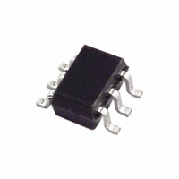
AD5601BKSZ-500RL7 Analog Devices Inc, AD5601BKSZ-500RL7 Datasheet - Page 3

AD5601BKSZ-500RL7
Manufacturer Part Number
AD5601BKSZ-500RL7
Description
IC DAC 8BIT BUFF V-OUT SC70-6
Manufacturer
Analog Devices Inc
Series
nanoDAC™r
Datasheet
1.AD5601BKSZ-REEL7.pdf
(20 pages)
Specifications of AD5601BKSZ-500RL7
Data Interface
Serial
Settling Time
6µs
Number Of Bits
8
Number Of Converters
1
Voltage Supply Source
Single Supply
Power Dissipation (max)
500µW
Operating Temperature
-40°C ~ 125°C
Mounting Type
Surface Mount
Package / Case
SC-70-6, SC-88, SOT-363
Resolution (bits)
8bit
Sampling Rate
1.7MSPS
Input Channel Type
Serial
Supply Voltage Range - Analog
2.7V To 5.5V
Supply Current
75µA
Digital Ic Case Style
SC-70
Number Of Channels
1
Resolution
8b
Conversion Rate
1.7MSPS
Interface Type
SER 3W SPI QSPI UW
Single Supply Voltage (typ)
3.3/5V
Dual Supply Voltage (typ)
Not RequiredV
Architecture
Resistor-String
Power Supply Requirement
Single
Output Type
Voltage
Integral Nonlinearity Error
±0.5+/- LSB
Single Supply Voltage (min)
2.7V
Single Supply Voltage (max)
5.5V
Dual Supply Voltage (min)
Not RequiredV
Dual Supply Voltage (max)
Not RequiredV
Operating Temp Range
-40C to 125C
Operating Temperature Classification
Automotive
Mounting
Surface Mount
Pin Count
6
Package Type
SC-70
Lead Free Status / RoHS Status
Lead free / RoHS Compliant
Lead Free Status / RoHS Status
Lead free / RoHS Compliant, Lead free / RoHS Compliant
Available stocks
Company
Part Number
Manufacturer
Quantity
Price
Part Number:
AD5601BKSZ-500RL7
Manufacturer:
ADI/亚德诺
Quantity:
20 000
SPECIFICATIONS
V
for A/B grades is −40°C to +125°C, typical at 25°C.
Table 2.
Parameter
STATIC PERFORMANCE
OUTPUT CHARACTERISTICS
LOGIC INPUTS
DD
AD5601
AD5611
AD5621
Zero-Code Error
Full-Scale Error
Offset Error
Gain Error
Zero-Code Error Drift
Gain Temperature Coefficient
Output Voltage Range
Output Voltage Settling Time
Slew Rate
Capacitive Load Stability
Output Noise Spectral Density
Noise
Digital-to-Analog Glitch Impulse
Digital Feedthrough
Short-Circuit Current
DC Output Impedance
Input Current
Input High Voltage, V
Input Low Voltage, V
Pin Input Capacitance
= 2.7 V to 5.5 V; R
Resolution
Relative Accuracy
Differential Nonlinearity (DNL)
Resolution
Relative Accuracy
Differential Nonlinearity (DNL)
Resolution
Relative Accuracy
Differential Nonlinearity (DNL)
3
1
1
1
INL
L
(INL)
INH
(INL)
(INL)
= 2 kΩ to GND; C
2
Min
10
12
0
1.8
1.4
L
= 200 pF to GND; all specifications T
Typ
0.5
±0.5
±0.063
±0.0004
6
1000
0.2
0.5
5.0
2.0
0.5
470
120
2
5
15
3
A Grade
Max
±4
±0.5
±6
±0.5
10
±10
±0.037
V
10
±2
0.8
0.6
DD
Rev. E | Page 3 of 20
Min
8
0
1.8
1.4
Typ
0.5
±0.5
±0.063
±0.0004
5.0
2.0
6
0.5
470
1000
120
2
5
0.2
15
0.5
3
B Grade
MIN
Max
±0.5
±0.5
±0.5
±0.5
±1
±0.5
10
±10
±0.037
V
10
±2
0.8
0.6
DD
to T
MAX
, unless otherwise noted. Temperature range
Unit
Bits
LSB
LSB
Bits
LSB
LSB
Bits
LSB
LSB
mV
mV
mV
%FSR
μV/°C
ppm
FSR/°C
V
μs
V/μs
pF
pF
nV/√Hz
μV
nV-s
nV-s
mA
Ω
μA
V
V
V
V
pF
AD5601/AD5611/AD5621
Test Conditions/Comments
Guaranteed monotonic by design
Guaranteed monotonic by design
Guaranteed monotonic by design
All 0s loaded to DAC register
All 1s loaded to DAC register
Code ¼ scale to ¾ scale
R
R
DAC code = midscale,1 kHz
DAC code = midscale,
0.1 Hz to 10 kHz bandwidth
1 LSB change around major carry
V
V
V
V
V
L
L
DD
DD
DD
DD
DD
= ∞
= 2 kΩ
= 3 V/5 V
= 4.7 V to 5.5 V
= 2.7 V to 3.6 V
= 4.7 V to 5.5 V
= 2.7 V to 3.6 V


