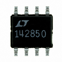
LTC1428CS8-50#PBF Linear Technology, LTC1428CS8-50#PBF Datasheet - Page 6

LTC1428CS8-50#PBF
Manufacturer Part Number
LTC1428CS8-50#PBF
Description
IC DAC 8BIT SINK OUT 8-SOIC
Manufacturer
Linear Technology
Datasheet
1.LTC1428CS8-50PBF.pdf
(8 pages)
Specifications of LTC1428CS8-50#PBF
Number Of Bits
8
Data Interface
Serial
Number Of Converters
1
Voltage Supply Source
Single Supply
Power Dissipation (max)
120µW
Operating Temperature
0°C ~ 70°C
Mounting Type
Surface Mount
Package / Case
8-SOIC (3.9mm Width)
Number Of Channels
1
Resolution
8b
Interface Type
SERIAL 1,2,3 WIRE
Single Supply Voltage (typ)
3.3V
Dual Supply Voltage (typ)
Not RequiredV
Power Supply Requirement
Single
Output Type
Current
Single Supply Voltage (min)
3V
Single Supply Voltage (max)
6.5V
Dual Supply Voltage (min)
Not RequiredV
Dual Supply Voltage (max)
Not RequiredV
Operating Temp Range
0C to 70C
Operating Temperature Classification
Commercial
Mounting
Surface Mount
Pin Count
8
Package Type
SOIC N
Resolution (bits)
8bit
Input Channel Type
Serial
Supply Current
130µA
Digital Ic Case Style
SOIC
No. Of Pins
8
Operating Temperature Range
0°C To +70°C
Msl
MSL 1 - Unlimited
Rohs Compliant
Yes
Lead Free Status / RoHS Status
Lead free / RoHS Compliant
Settling Time
-
Lead Free Status / Rohs Status
Compliant
Available stocks
Company
Part Number
Manufacturer
Quantity
Price
SERIAL I/O OPERATI G SEQUE CE
D
LTC1428-50
8-BIT CURRENT OUTPUT DAC
The LTC1428-50 is an 8-bit, current sink output digital-to-
analog (DAC) converter. The LTC1428-50 is guaranteed
monotonic and is digitally adjustable in 256 equal steps.
Upon power up, the counter resets to 1000000B and the
DAC output assumes midrange. The I
from 2V to 10V. The LTC1428-50 features a full-scale
output current of 50 A 3% at room temperature ( 5%
over temperature). This device also includes a flexible
serial digital interface that allows easy interconnection to
a variety of digital systems.
DIGITAL INTERFACE
Automatic Mode Selection
The LTC1428-50 includes a serial interface capable of com-
municating with the host system using one of three pro-
tocols; standard 3-wire mode, a 2-wire up/down pulse mode
and a 1-wire increment-only pulse mode. The LTC1428-50
is designed to autoconfigure itself depending on the method
6
APPLICATIONS
CLK
OUT
D
CS
IN
Hi-Z
3-WIRE MODE
t
t
CSS
CKS
CS GOES
Figure 2. LTC1428-50 Operating Modes
t
LOW
DV
D7
D7
D
INCREMENT/
DECREMENT
POWER-UP
GOES LOW
IN
U
(UP/DN)
D6
INFORMATION
U
D6
PULSE MODE
CS STAYS
HIGH
U
D5
W
OUT
INCREMENT-
Figure 1. 3-Wire Interface Timing Specification
D
HIGH
t
D5
DS
IN
pin can be biased
ONLY
STAYS
D4
1428-50 F02
U
D4
U
t
DH
t
CSLO
D3
D3
of data presentation. A diagram illustrating this
autodetection behavior is shown in Figure 2. At power-up,
the interface is set to 1-wire pulse mode. If the CS line ever
goes low (as it will at the beginning of a valid 3-wire serial
transfer) the chip immediately reconfigures itself into 3-wire
mode and remains in this mode until power is cycled. If CS
stays high, the device stays in pulse mode and monitors the
UP/DN pin to determine whether to switch to 2-wire mode.
If UP/DN ever goes low (as it will the first time a “down”
command is given) the chip switches into 2-wire pulse
mode and remains in this mode until power is cycled. In a
properly configured 1-wire system, CS and UP/DN will
always remain high. 2-wire pulse mode systems must
provide a single logic low pulse before the first data pulses
are sent to prevent the LTC1428-50 from remaining in
1-wire mode if the first several pulses are logic high.
Standard 3-Wire Mode (Figure 3)
Refer to the Serial Interface Operating Sequence in Figure
1. When operating in 3-wire mode, the LTC1428-50 will
interface directly with most standard 3- or 4-wire serial
interface systems. The clock (CLK) input synchronizes the
data transfer with each input bit captured at the rising edge
of CLK and each output data bit shifted through D
falling edge. Data is shifted into and out of the LTC1428-
50 starting with the MSB bit. A falling edge at CS initiates
the data transfer and brings the D
The serial 8-bit data representing the new DAC setting is
shifted into the D
setting is shifted out of the D
t
DO
D2
D2
t
CKHI
IN
D1
pin. Simultaneously, the previous DAC
t
D1
CKLO
OUT
D0
D0
OUT
pin. After the new data is
pin out of three-state.
t
CKH
t
CSH
D7
t
DZ
t
CSHI
OUT
Hi-Z
at the
1428-50 F01


