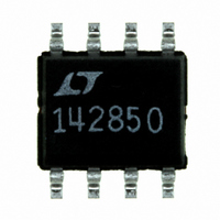
LTC1428CS8-50#PBF Linear Technology, LTC1428CS8-50#PBF Datasheet - Page 4

LTC1428CS8-50#PBF
Manufacturer Part Number
LTC1428CS8-50#PBF
Description
IC DAC 8BIT SINK OUT 8-SOIC
Manufacturer
Linear Technology
Datasheet
1.LTC1428CS8-50PBF.pdf
(8 pages)
Specifications of LTC1428CS8-50#PBF
Number Of Bits
8
Data Interface
Serial
Number Of Converters
1
Voltage Supply Source
Single Supply
Power Dissipation (max)
120µW
Operating Temperature
0°C ~ 70°C
Mounting Type
Surface Mount
Package / Case
8-SOIC (3.9mm Width)
Number Of Channels
1
Resolution
8b
Interface Type
SERIAL 1,2,3 WIRE
Single Supply Voltage (typ)
3.3V
Dual Supply Voltage (typ)
Not RequiredV
Power Supply Requirement
Single
Output Type
Current
Single Supply Voltage (min)
3V
Single Supply Voltage (max)
6.5V
Dual Supply Voltage (min)
Not RequiredV
Dual Supply Voltage (max)
Not RequiredV
Operating Temp Range
0C to 70C
Operating Temperature Classification
Commercial
Mounting
Surface Mount
Pin Count
8
Package Type
SOIC N
Resolution (bits)
8bit
Input Channel Type
Serial
Supply Current
130µA
Digital Ic Case Style
SOIC
No. Of Pins
8
Operating Temperature Range
0°C To +70°C
Msl
MSL 1 - Unlimited
Rohs Compliant
Yes
Lead Free Status / RoHS Status
Lead free / RoHS Compliant
Settling Time
-
Lead Free Status / Rohs Status
Compliant
Available stocks
Company
Part Number
Manufacturer
Quantity
Price
TYPICAL PERFORMANCE CHARACTERISTICS
I
systems, the DAC I
V
must be kept free from noise and ripple by bypassing
directly to a ground plane.
SHDN (Pin 3): Shutdown. A logic low puts the chip
into shutdown mode. The digital setting for the DAC is
retained.
CLK (Pin 4): Shift Clock. This clock synchronizes the serial
data and has a Schmitt trigger input.
CS (Pin 5): Chip Select Input. In 3-wire mode, a logic low
enables the LTC1428-50. Upon power-up, a logic high
LTC1428-50
4
PIN
OUT
CC
52.5
51.5
48.5
50.5
49.5
47.5
U
(Pin 2): Voltage Supply (3V V
– 55
(Pin 1): DAC Current Sink Output. In 3.3V or 5V
Temperature Variation
V
V(I
FUNCTIONS
CC
OUT
– 25
= 3.3V
) = 2.5V
U
5
TEMPERATURE ( C)
35
OUT
U
65
pin can be biased from 2V to 10V.
95
W
125
1428-50 G04
U
CC
155
6.5V). This supply
–10
–12
– 6
– 8
–2
–4
2
0
Bias Voltage Rejection
0
2
4
I
OUT
6
BIAS VOLTAGE (V)
8
puts the chip into pulse mode. If CS ever goes low, the chip
is configured into 3-wire mode until V
GND (Pin 6): Ground. Ground should be tied directly to a
ground plane.
D
data is shifted into D
logic high puts the counter into increment-only mode. If
D
decrement mode until V
D
conversion D
data. In pulse mode, D
10
IN
IN
OUT
ever goes low, the counter is configured in increment/
(UP/DN)(Pin 7): Data Input. In 3-wire mode, the DAC
V
T
12
A
CC
= 25 C
(Pin 8): Data Output. In 3-wire mode, on every
= 3.3V
1428-50 G05
14
16
OUT
0.06
0.05
0.04
0.03
0.02
0.01
0
serially outputs the previous 8-bit DAC
IN
. In pulse mode, upon power-up a
OUT
CC
20
18
16
14
12
10
8
6
4
2
0
0
Zero-Scale I
is three-stated.
is reset.
V
CC
10
= 3.3V
20
TEMPERATURE ( C)
OUT
CC
30
vs Temperature
is reset.
V(I
40
OUT
) = 10V
V(I
50
V(I
OUT
OUT
) = 2.5V
) = 5V
60
1428-50 G06
70


