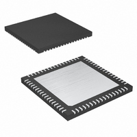
MAX5888AEGK+D Maxim Integrated Products, MAX5888AEGK+D Datasheet - Page 17

MAX5888AEGK+D
Manufacturer Part Number
MAX5888AEGK+D
Description
IC DAC 16BIT 3.3V 500MSPS 68-QFN
Manufacturer
Maxim Integrated Products
Datasheet
1.MAX5888AEGKD.pdf
(18 pages)
Specifications of MAX5888AEGK+D
Settling Time
11ns
Number Of Bits
16
Data Interface
Parallel
Number Of Converters
1
Voltage Supply Source
Analog and Digital
Power Dissipation (max)
130mW
Operating Temperature
-40°C ~ 85°C
Mounting Type
Surface Mount
Package / Case
68-QFN Exposed Pad
Lead Free Status / RoHS Status
Lead free / RoHS Compliant
The offset error is the difference between the ideal and
the actual offset current. For a DAC, the offset point is
the value at the output for the two midscale digital input
codes with respect to the full scale of the DAC. This
error affects all codes by the same amount.
A gain error is the difference between the ideal and the
actual full-scale output voltage on the transfer curve,
after nullifying the offset error. This error alters the slope
of the transfer function and corresponds to the same
percentage error in each step.
The settling time is the amount of time required from the
start of a transition until the DAC output settles its new
output value to within the converter’s specified accuracy.
Glitch impulses are caused by asymmetrical switching
times in the DAC architecture, which generates unde-
sired output transients. The amount of energy that
appears at the DAC’s output is measured over time and
usually specified in the pV-s range.
For a waveform perfectly reconstructed from digital sam-
ples, the theoretical maximum SNR is the ratio of the full-
scale analog output (RMS value) to the RMS quantization
error (residual error). The ideal, theoretical minimum can
be derived from the DAC’s resolution (N bits):
However, noise sources such as thermal noise, refer-
ence noise, clock jitter, etc., affect the ideal reading;
therefore, SNR is computed by taking the ratio of the
RMS signal to the RMS noise, which includes all spec-
tral components minus the fundamental, the first four
harmonics, and the DC offset.
Performance DAC with Differential LVDS Inputs
Dynamic Performance Parameter
SNR
dB
______________________________________________________________________________________
= 6.02
Signal-to-Noise Ratio (SNR)
dB
3.3V, 16-Bit, 500Msps High Dynamic
✕
N + 1.76
dB
Glitch Energy
Settling Time
Definitions
Offset Error
Gain Error
SFDR is the ratio of RMS amplitude of the carrier fre-
quency (maximum signal components) to the RMS
value of their next-largest distortion component. SFDR
is usually measured in dBc and with respect to the car-
rier frequency amplitude or in dB FS with respect to the
DAC’s full-scale range. Depending on its test condition,
SFDR is observed within a predefined window or
to Nyquist.
The two-tone IMD is the ratio expressed in dBc (or dB
FS) of either input tone to the worst 3rd-order (or high-
er) IMD products. Note that 2nd-order IMD products
usually fall at frequencies that can be easily removed
by digital filtering; therefore, they are not as critical as
3rd-order IMDs. The two-tone IMD performance of the
MAX5888 was tested with the two individual input tone
levels set to at least -6dB FS and the four-tone perfor-
mance was tested according to the GSM model at an
output frequency of 32MHz and amplitude of -12dB FS.
Commonly used in combination with WCDMA, ACLR
reflects the leakage power ratio in dB between the
measured power within a channel relative to its adja-
cent channel. ACLR provides a quantifiable method of
determining out-of-band spectral energy and its influ-
ence on an adjacent channel when a bandwidth-limited
RF signal passes through a nonlinear device.
TRANSISTOR COUNT: 10,629
PROCESS: CMOS
Two-/Four-Tone Intermodulation
Spurious-Free Dynamic Range (SFDR)
Adjacent Channel Leakage
Chip Information
Power Ratio (ACLR)
Distortion (IMD)
17


