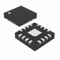
MAX5138BGTE+ Maxim Integrated Products, MAX5138BGTE+ Datasheet - Page 9

MAX5138BGTE+
Manufacturer Part Number
MAX5138BGTE+
Description
IC DAC 16BIT SGL 16-TQFN
Manufacturer
Maxim Integrated Products
Datasheet
1.MAX5139GTE.pdf
(17 pages)
Specifications of MAX5138BGTE+
Settling Time
5µs
Number Of Bits
16
Data Interface
DSP, I²C, MICROWIRE™, Parallel, QSPI™, SPI™
Number Of Converters
1
Voltage Supply Source
Analog and Digital
Operating Temperature
-40°C ~ 105°C
Mounting Type
Surface Mount
Package / Case
16-TQFN Exposed Pad
Interface Type
Serial (SPI, QSPI, Microwire, DSP)
Supply Voltage (max)
5.25 V
Supply Voltage (min)
2.7 V
Maximum Operating Temperature
+ 105 C
Mounting Style
SMD/SMT
Maximum Power Dissipation
1176.5 mW
Minimum Operating Temperature
- 40 C
Supply Current
1 mA
Lead Free Status / RoHS Status
Lead free / RoHS Compliant
Power Dissipation (max)
-
Lead Free Status / Rohs Status
Lead free / RoHS Compliant
The MAX5138/MAX5139 are a family of single-channel,
pin-compatible and software-compatible, 16-bit and 12-
bit DACs. The parts are low-power, buffered voltage-
output, high-linearity DACs. The MAX5138/MAX5139
minimize the digital noise feedthrough from input to out-
put by powering down the SCLK and DIN input buffers
after completion of each 24-bit serial input. On power-
up, the MAX5138/MAX5139 reset the DAC output to zero
or midscale, depending on the state of the M/Z input,
providing additional safety for applications that drive
valves or other transducers that need to be off on power-
up. The MAX5138/MAX5139 contain a segmented resis-
tor string-type DAC, a serial-in parallel-out shift register,
a DAC register, power-on reset (POR) circuit, and con-
trol logic. On the falling edge of the clock (SCLK) pulse,
the serial input (DIN) data is shifted into the device, MSB
first. During power-down, an internal 80kΩ resistor pulls
DAC outputs to AGND.
1, 4, 9
PIN
10
11
12
13
14
15
16
—
2
3
5
6
7
8
_______________________________________________________________________________________
READY
NAME
AGND
AGND
DVDD
AVDD
LDAC
SCLK
REFO
N.C.
OUT
REFI
M/Z
DIN
CS
EP
Detailed Description
No Connection. Not internally connected.
Power-Up Reset Select. Connect M/Z low to AGND to power up the DAC output. Connect M/Z
high to power up the DAC output to midscale.
Load DAC. Active-low hardware load DAC input.
Serial-Clock Input
Active-Low Chip-Select Input
Data In
Analog Ground. Internally connected to AGND. Connect AGND to AGND externally.
Data Output
Digital Power Supply. Bypass DVDD with a 0.1µF capacitor to AGND.
Buffered DAC Output
Analog Power Supply. Bypass AVDD with a 0.1µF capacitor to AGND.
Reference Voltage Input. Bypass REFI with a 0.1µF capacitor to AGND.
Reference Voltage Output
DAC Ground. Internally connected to AGND. Connect AGND to AGND externally.
Exposed Pad. Not internally connected. Connect to a ground or leave unconnected. Not intended
as an electrical connection point.
Buffered Voltage-Output DACs
Low-Power, Single, 16-/12-Bit,
The MAX5138/MAX5139 include an internal buffer for the
DAC output. The internal buffer provides improved load
regulation and transition glitch suppression for the DAC
output. The output buffer slews at 1.25V/µs and drives up
to 2kΩ in parallel with 200pF. The analog supply voltage
(AVDD) determines the maximum output voltage range
of the device as AVDD powers the output buffer.
The MAX5138/MAX5139 feature an internal reference
with a nominal +2.44V output. Connect REFO to REFI
when using the internal reference. Bypass REFO to
AGND with a 47pF (maximum 100pF) capacitor.
Alternatively, if heavier decoupling is required, add a
1kΩ resistor in series with a 1µF capacitor in parallel
with the existing 100pF capacitor. REFO can deliver up
to 100µA of current with no degradation in perfor-
mance. Configure other reference voltages by applying
a resistive potential divider with a total resistance
greater than 33kΩ from REFO to AGND.
FUNCTION
Output Amplifier (OUT)
Pin Description
DAC Reference
Internal Reference
9


