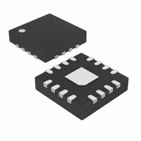
MAX5138BGTE+ Maxim Integrated Products, MAX5138BGTE+ Datasheet

MAX5138BGTE+
Specifications of MAX5138BGTE+
Related parts for MAX5138BGTE+
MAX5138BGTE+ Summary of contents
Page 1
... Than ±10mV) o 30MHz 3-Wire SPI-/QSPI-/MICROWIRE-/ DSP-Compatible Serial Interface o CMOS-Compatible Inputs with Hysteresis o Low Power Consumption (I PART MAX5138BGTE+ MAX5139GTE+ + Denotes a lead(Pb)-free/RoHS-compliant package Exposed pad. Applications Note: All devices are specified over the -40°C to +105°C operating temperature range. ...
Page 2
Low-Power, Single, 16-/12-Bit, Buffered Voltage-Output DACs ABSOLUTE MAXIMUM RATINGS AVDD to AGND ........................................................-0.3V to +6V DVDD to AGND ........................................................-0.3V to +6V OUT to AGND...............................................-0.3V to the lower of REFI, REFO, M/Z to AGND ...........................-0.3V to the lower of SCLK, DIN, ...
Page 3
ELECTRICAL CHARACTERISTICS (continued 2.7V to 5.25V 2.7V to 5.25V, V AVDD DVDD unless otherwise noted. Typical values are MIN MAX PARAMETER SYMBOL DAC OUTPUT VOLTAGE (Note 2) ...
Page 4
Low-Power, Single, 16-/12-Bit, Buffered Voltage-Output DACs ELECTRICAL CHARACTERISTICS (continued 2.7V to 5.25V 2.7V to 5.25V, V AVDD DVDD unless otherwise noted. Typical values are MIN MAX PARAMETER ...
Page 5
A MAX5138 INTEGRAL NONLINEARITY vs. DIGITAL INPUT CODE 16,384 32,768 49,152 65,536 DIGITAL INPUT CODE (LSB) DIFFERENTIAL NONLINEARITY vs. DIGITAL INPUT CODE 1.0 0.8 0.6 0.4 ...
Page 6
Low-Power, Single, 16-/12-Bit, Buffered Voltage-Output DACs (T = +25°C, unless otherwise noted.) A OFFSET ERROR vs. TEMPERATURE 0.8 0.6 0.4 0 5.25V AVDD REF -0.2 -0.4 -0 2.7V AVDD -0 ...
Page 7
A SETTLING TIME DOWN 400ns/div DIGITAL SUPPLY CURRENT vs. DIGITAL SUPPLY VOLTAGE 0. 5.25V AVDD 0. 1MHz SCLK 0.40 0.35 0.30 0.25 0.20 0.15 0.10 0.05 0 2.7 3.2 3.7 ...
Page 8
Low-Power, Single, 16-/12-Bit, Buffered Voltage-Output DACs (T = +25°C, unless otherwise noted.) A FULL-SCALE REFERENCE FEEDTHROUGH V OUT V REF 20μs/div REFERENCE INPUT RESPONSE vs. FREQUENCY 0 -5 -10 -15 -20 -25 -30 - 100 1000 10,000 INPUT ...
Page 9
PIN NAME N.C. No Connection. Not internally connected. Power-Up Reset Select. Connect M/Z low to AGND to power up the DAC output. Connect M/Z 2 M/Z high to power up the DAC output to midscale. LDAC 3 ...
Page 10
Low-Power, Single, 16-/12-Bit, Buffered Voltage-Output DACs The external reference input features a typical input impedance of 113kΩ and accepts an input voltage from +2V to AVDD. Connect an external voltage supply between REFI and AGND to apply an ex- ternal ...
Page 11
The MAX5138’s DAC code is unipolar binary with V = (code/65536 See Table 1 for the serial inter- REF face commands. The MAX5139’s DAC code is unipolar with V (code/4096 See Table 1 for ...
Page 12
Low-Power, Single, 16-/12-Bit, Buffered Voltage-Output DACs Daisy chain multiple MAX5138/MAX5139 devices by connecting the first device conventionally, then connect its READY output to the CS of the following device. Repeat for any other devices in the chain, and drive the ...
Page 13
CSm μC CS1 CS SCLK DWRITE DREAD INT Figure 6. Daisy Chain (CS Not Used) LDAC OUT Figure 7. Output Timing ______________________________________________________________________________________ Low-Power, Single, 16-/12-Bit, Buffered Voltage-Output DACs TO OTHER CHIPS/CHAINS t LDACPWL t S SLAVE 1 CS SCLK MAX5138 ...
Page 14
Low-Power, Single, 16-/12-Bit, Buffered Voltage-Output DACs Applications Information Power-On Reset (POR) On power-up, the input register is set to zero, and the DAC output powers up to zero or midscale, depending on the configuration of M/Z. Connect M/Z to AGND ...
Page 15
Offset error indicates how well the actual transfer func- tion matches the ideal transfer function at a single point. Typically, the point at which the offset error is specified near the zero-scale point of the transfer function. ...
Page 16
Low-Power, Single, 16-/12-Bit, Buffered Voltage-Output DACs DIGITAL POWER SUPPLY 100nF *SHOWN IN BIPOLAR CONFIGURATION Package Information For the latest package outline information and land patterns www.maxim-ic.com/packages. PACKAGE TYPE PACKAGE CODE 16 TQFN-EP T1633-5 16 ______________________________________________________________________________________ ANALOG POWER SUPPLY ...
Page 17
... Maxim cannot assume responsibility for use of any circuitry other than circuitry entirely embodied in a Maxim product. No circuit patent licenses are implied. Maxim reserves the right to change the circuitry and specifications without notice at any time. Maxim Integrated Products, 120 San Gabriel Drive, Sunnyvale, CA 94086 408-737-7600 ____________________ 17 © 2009 Maxim Integrated Products ...


