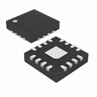
MAX5138BGTE+ Maxim Integrated Products, MAX5138BGTE+ Datasheet - Page 14

MAX5138BGTE+
Manufacturer Part Number
MAX5138BGTE+
Description
IC DAC 16BIT SGL 16-TQFN
Manufacturer
Maxim Integrated Products
Datasheet
1.MAX5139GTE.pdf
(17 pages)
Specifications of MAX5138BGTE+
Settling Time
5µs
Number Of Bits
16
Data Interface
DSP, I²C, MICROWIRE™, Parallel, QSPI™, SPI™
Number Of Converters
1
Voltage Supply Source
Analog and Digital
Operating Temperature
-40°C ~ 105°C
Mounting Type
Surface Mount
Package / Case
16-TQFN Exposed Pad
Interface Type
Serial (SPI, QSPI, Microwire, DSP)
Supply Voltage (max)
5.25 V
Supply Voltage (min)
2.7 V
Maximum Operating Temperature
+ 105 C
Mounting Style
SMD/SMT
Maximum Power Dissipation
1176.5 mW
Minimum Operating Temperature
- 40 C
Supply Current
1 mA
Lead Free Status / RoHS Status
Lead free / RoHS Compliant
Power Dissipation (max)
-
Lead Free Status / Rohs Status
Lead free / RoHS Compliant
Low-Power, Single, 16-/12-Bit,
Buffered Voltage-Output DACs
On power-up, the input register is set to zero, and the
DAC output powers up to zero or midscale, depending
on the configuration of M/Z. Connect M/Z to AGND to
power the output to AGND. Connect M/Z to AVDD to
power the output to midscale.
To guarantee DAC linearity, wait until the supplies have
settled. Set the LIN bit in the DAC linearity register; wait
10ms, and clear the LIN bit.
The MAX5138/MAX5139 unipolar output voltage range is
0 to V
with 200pF.
Use the MAX5138/MAX5139 in bipolar applications with
additional external components (see the Typical
Operating Circuit ).
For best performance, use a separate supply for the
MAX5138/MAX5139. Bypass both DVDD and AVDD
with high-quality ceramic capacitors to a low-imped-
ance ground as close as possible to the device.
Minimize lead lengths to reduce lead inductance.
Connect both MAX5138/MAX5139 AGND inputs to the
analog ground plane.
Table 2. MAX5138 Input Code vs. Output
Voltage
14
DAC LATCH CONTENTS
MSB
1111 1111 1111 1111
1000 0000 0000 0000
0000 0000 0000 0001
0000 0000 0000 0000
______________________________________________________________________________________
REFI
. The output buffer drives a 2kΩ load in parallel
Applications Information
LSB
Bypassing Considerations
V
V
V
0
REF
REF
REF
Power-On Reset (POR)
ANALOG OUTPUT, V
x (65,535/65,536)
x (32,768/65,536) = 1/2 V
x (1/65,536)
Power Supplies and
Unipolar Output
Bipolar Output
OUT
REF
Digital and AC transient signals on AGND inputs can
create noise at the outputs. Connect both AGND inputs
to form the star ground for the DAC system. Refer
remote DAC loads to this system ground for the best
possible performance. Use proper grounding tech-
niques, such as a multilayer board with a low-induc-
tance ground plane, or star connect all ground return
paths back to the MAX5138/MAX5139 AGND. Do not
use wire-wrapped boards and sockets. Use shielding
to improve noise immunity. Do not run analog and digi-
tal signals parallel to one another (especially clock sig-
nals) and avoid routing digital lines underneath the
MAX5138/MAX5139 package.
INL is the deviation of the measured transfer function
from a best fit straight line drawn between two codes.
This best fit line for the MAX5138 is a line drawn
between codes 3072 and 64,512 of the transfer func-
tion and the best fit line for the MAX5139 is a line drawn
between codes 192 and 4032 of the transfer function,
once offset and gain errors have been nullified.
DNL is the difference between an actual step height
and the ideal value of 1 LSB. If the magnitude of the
DNL is greater than -1 LSB, the DAC guarantees no
missing codes and is monotonic.
Table 3. MAX5139 Input Code vs. Output
Voltage
DAC LATCH CONTENTS
MSB
1111 1111 1111 XXX
1000 0000 0000 XXX
0000 0000 0001 XXX
0000 0000 0000 XXX
Differential Nonlinearity (DNL)
LSB
Integral Nonlinearity (INL)
Layout Considerations
V
V
V
0
REF
REF
REF
ANALOG OUTPUT, V
x (4095/4096)
x (2048/4096)
x (1/4096)
Definitions
OUT


