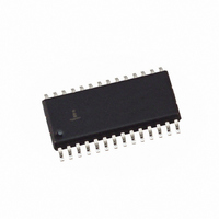
HI5741BIB Intersil, HI5741BIB Datasheet - Page 11

HI5741BIB
Manufacturer Part Number
HI5741BIB
Description
IC DAC 14-BIT 100MSPS 28-SOIC
Manufacturer
Intersil
Datasheet
1.HI5741BIB.pdf
(13 pages)
Specifications of HI5741BIB
Settling Time
20ns
Number Of Bits
14
Data Interface
Parallel
Number Of Converters
1
Voltage Supply Source
Analog and Digital, Dual ±
Power Dissipation (max)
650mW
Operating Temperature
-40°C ~ 85°C
Mounting Type
Surface Mount
Package / Case
28-SOIC (7.5mm Width)
Lead Free Status / RoHS Status
Contains lead / RoHS non-compliant
Available stocks
Company
Part Number
Manufacturer
Quantity
Price
Company:
Part Number:
HI5741BIB
Manufacturer:
HARRIS
Quantity:
91
Part Number:
HI5741BIB
Manufacturer:
INTERSIL
Quantity:
20 000
Company:
Part Number:
HI5741BIBZ
Manufacturer:
Intersil
Quantity:
126
to change before another. In order to minimize this, the
Intersil HI5741 employs an internal register, just prior to the
current sources, which is updated on the clock edge. Lastly,
the worst case glitch on traditional D/A converters usually
occurs at the major transition (i.e., code 8191 to 8192).
However, due to the split architecture of the HI5741, the
glitch is moved to the 1023 to 1024 transition (and every
subsequent 1024 code transitions thereafter). This split
R/2R segmented current source architecture, which
decreases the amount of current switching at any one time,
makes the glitch practically constant over the entire output
range. By making the glitch a constant size over the entire
output range this effectively integrates this error out of the
end application.
In measuring the output glitch of the HI5741 the output is
terminated into a 64Ω load. The glitch is measured at any
one of the current cell carry (code 1023 to 1024 transition or
any multiple thereof) throughout the DACs output range.
The glitch energy is calculated by measuring the area under
the voltage-time curve. Figure 25 shows the area considered
as glitch when changing the DAC output. Units are typically
specified in picoVolt/seconds (pV/s).
Applications
Bipolar Applications
To convert the output of the HI5741 to a bipolar 4V swing,
the following applications circuit is recommended. The
reference can only provide 125µA of drive, so it must be
buffered to create the bipolar offset current needed to
generate the -2V output with all bits ‘off’. The output current
must be converted to a voltage and then gained up and
offset to produce the proper swing. Care must be taken to
compensate for the voltage swing and error.
a
(mV)
FIGURE 25. MEASURING GLITCH ENERGY
HI5741
FIGURE 24. GLITCH TEST CIRCUIT
(21) I
OUT
t
(ns)
64Ω
11
GLITCH ENERGY = (
LOW PASS
100MHz
FILTER
SCOPE
a
50Ω
x
t
)/2
HI5741
Interfacing to the HSP45106 NCO-16
The HSP45106 is a 16-bit Numerically Controlled Oscillator
(NCO). The HSP45106 can be used to generate various
modulation schemes for Direct Digital Synthesis (DDS)
applications. Figure 27 shows how to interface an HI5741 to
the HSP45106.
Definition of Specifications
Integral Linearity Error (INL) is the measure of the worst
case point that deviates from a best fit straight line of data
values along the transfer curve.
Differential Linearity Error (DNL) is the measure of the error
in step size between adjacent codes along the converter’s
transfer curve. Ideally, the step size is 1 LSB from one code to
the next, and the deviation from 1 LSB is known as DNL. A
DNL specification of greater than -1 LSB guarantees
monotonicity.
Feedthru is the measure of the undesirable switching noise
coupled to the output.
Output Voltage Full Scale Settling Time is the time
required from the 50% point on the clock input for a full scale
step to settle within an ±
Output Voltage Small Scale Settling Time is the time
required from the 50% point on the clock input for a 100mV
step to settle within an
applications reconstructing highly correlated signals such as
sine waves with more than 5 points per cycle.
Glitch Area (GE) is the switching transient appearing on the
output during a code transition. It is measured as the area
under the curve and expressed as a volt • time specification
(typically pV-s).
Differential Gain (∆A
wave with a normalized amplitude.
Differential Phase (∆Φ) is the phase error from an ideal sine
wave.
REF OUT
HI5741
I
OUT
(21)
(26)
FIGURE 26. BIPOLAR OUTPUT CONFIGURATION
1
/
2
CA2904
-
+
50Ω
V
1
) is the gain error from an ideal sine
5kΩ
/
1
2
/
2
LSB error band. This is used by
LSB error band.
0.1µF
1
/
2
+
CA2904
-
5kΩ
September 20, 2006
60Ω
240Ω
240Ω
HFA1100
+
-
FN4071.12
V
OUT


