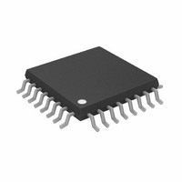
AD5763CSUZ Analog Devices Inc, AD5763CSUZ Datasheet - Page 4

AD5763CSUZ
Manufacturer Part Number
AD5763CSUZ
Description
DAC 16BIT DUAL 5V 2LSB 32-TQFP
Manufacturer
Analog Devices Inc
Datasheet
1.AD5763CSUZ.pdf
(28 pages)
Specifications of AD5763CSUZ
Data Interface
Serial
Design Resources
High Accuracy, Bipolar Voltage Output Digital-to-Analog Conversion Using AD5763 (CN0074)
Settling Time
8µs
Number Of Bits
16
Number Of Converters
2
Voltage Supply Source
Dual ±
Power Dissipation (max)
45mW
Operating Temperature
-40°C ~ 105°C
Mounting Type
Surface Mount
Package / Case
32-TQFP, 32-VQFP
Resolution (bits)
16bit
Input Channel Type
Serial
Supply Voltage Range - Analogue
4.75V To 5.25V
Supply Voltage Range - Digital
2.7V To 5.25V
Supply
RoHS Compliant
Lead Free Status / RoHS Status
Lead free / RoHS Compliant
Available stocks
Company
Part Number
Manufacturer
Quantity
Price
Company:
Part Number:
AD5763CSUZ
Manufacturer:
Analog Devices Inc
Quantity:
135
Company:
Part Number:
AD5763CSUZ
Manufacturer:
Analog Devices Inc
Quantity:
10 000
Company:
Part Number:
AD5763CSUZ-REEL7
Manufacturer:
Analog Devices Inc
Quantity:
10 000
AD5763
SPECIFICATIONS
AV
DV
Table 2.
Parameter
ACCURACY
REFERENCE INPUT
OUTPUT CHARACTERISTICS
DIGITAL INPUTS
DIGITAL OUTPUTS (D0, D1, SDO)
Resolution
Relative Accuracy (INL)
Differential Nonlinearity (DNL)
Bipolar Zero Error
Bipolar Zero Temperature
Coefficient (TC)
Zero-Scale Error
Zero-Scale Temperature Coefficient
(TC)
Gain Error
Gain Temperature Coefficient (TC)
DC Crosstalk
Reference Input Voltage
DC Input Impedance
Input Current
Reference Range
Output Voltage Range
Output Voltage Drift vs. Time
Short-Circuit Current
Load Current
Capacitive Load Stability
DC Output Impedance
Input High Voltage, V
Input Low Voltage, V
Input Current
Pin Capacitance
Output Low Voltage
Output High Voltage
Output Low Voltage
Output High Voltage
High Impedance Leakage Current
High Impedance Output
DD
CC
R
R
Capacitance
= 4.75 V to 5.25 V, AV
= 2.7 V to 5.25 V, R
LOAD
LOAD
1
= ∞
= 10 kΩ
1
1
1
1
IL
IH
2
LOAD
1
SS
= 5 kΩ, C
= −5.25 V to −4.75 V, AGNDx = DGND = REFGND = PGND = 0 V, REFA = REFB = 2.048 V,
1
1
LOAD
−1
Min
16
−1
−2
−3
−2
−3.5
−0.03
−0.04
1
1
−4.31158
−4.20103
−4.096
−4.42105
−1
2
−1
DV
DV
= 200 pF. All specifications T
CC
CC
− 1
− 0.5
Typ
±1
±1
±1
2.048
0.03
±32
±37
10
±1
5
Rev. A | Page 4 of 28
Max
+1
+1
+2
+3
+2
+3.5
+0.03
+0.04
0.5
10
2.1
+4.31158
+4.20103
+4.096
+4.42105
+1
200
1000
0.3
0.8
+1
10
0.4
0.4
MIN
Unit
Bits
LSB
LSB
mV
mV
ppm FSR/°C
mV
mV
ppm FSR/°C
% FSR
% FSR
ppm FSR/°C
LSB
V nominal
MΩ
μA
V
V
V
V
V
ppm FSR/500 hrs
ppm FSR/1000 hrs
mA
mA
pF
pF
Ω
V
V
μA
pF
V
V
V
V
μA
pF
to T
MAX
, unless otherwise noted.
Test Conditions/Comments
Outputs unloaded
Guaranteed monotonic
At 25°C
At 25°C
At 25°C, coarse gain register = 0
Coarse gain register = 0
±1% for specified performance
Typically 100 MΩ
Coarse gain register = 2
Coarse gain register = 1
Coarse gain register = 0
REFA = REFB = 2.1 V, coarse gain register = 2
RI
For specified performance
JEDEC compliant
Per pin
Per pin
DV
DV
DV
DV
SDO only
SDO only
SCC
CC
CC
CC
CC
= 6 kΩ, see Figure 23
= 5 V ± 5%, sinking 200 μA
= 5 V ± 5%, sourcing 200 μA
= 2.7 V to 3.6 V, sourcing 200 μA
= 2.7 V to 3.6 V, sinking 200 μA


