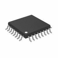
AD5763CSUZ Analog Devices Inc, AD5763CSUZ Datasheet - Page 24

AD5763CSUZ
Manufacturer Part Number
AD5763CSUZ
Description
DAC 16BIT DUAL 5V 2LSB 32-TQFP
Manufacturer
Analog Devices Inc
Datasheet
1.AD5763CSUZ.pdf
(28 pages)
Specifications of AD5763CSUZ
Data Interface
Serial
Design Resources
High Accuracy, Bipolar Voltage Output Digital-to-Analog Conversion Using AD5763 (CN0074)
Settling Time
8µs
Number Of Bits
16
Number Of Converters
2
Voltage Supply Source
Dual ±
Power Dissipation (max)
45mW
Operating Temperature
-40°C ~ 105°C
Mounting Type
Surface Mount
Package / Case
32-TQFP, 32-VQFP
Resolution (bits)
16bit
Input Channel Type
Serial
Supply Voltage Range - Analogue
4.75V To 5.25V
Supply Voltage Range - Digital
2.7V To 5.25V
Supply
RoHS Compliant
Lead Free Status / RoHS Status
Lead free / RoHS Compliant
Available stocks
Company
Part Number
Manufacturer
Quantity
Price
Company:
Part Number:
AD5763CSUZ
Manufacturer:
Analog Devices Inc
Quantity:
135
Company:
Part Number:
AD5763CSUZ
Manufacturer:
Analog Devices Inc
Quantity:
10 000
Company:
Part Number:
AD5763CSUZ-REEL7
Manufacturer:
Analog Devices Inc
Quantity:
10 000
AD5763
APPLICATIONS INFORMATION
TYPICAL OPERATING CIRCUIT
Figure 29 shows the typical operating circuit for the AD5763.
The only external components needed for this precision 16-bit
DAC are a reference voltage source, decoupling capacitors on
the supply pins and reference inputs, and an optional short-
circuit current setting resistor. Because the device incorporates
reference buffers, it eliminates the need for an external bipolar
reference and associated buffers. This leads to overall savings in
both cost and board space.
In Figure 29, AV
to −5 V and AGNDA and AGNDB are connected to REFGND.
DD
is connected to +5 V and AV
BIN/2sCOMP
RSTOUT
RSTIN
SYNC
LDAC
SCLK
SDIN
SDO
D0
D1
SS
is connected
NC = NO CONNECT
+5V
100nF
10µF
Figure 29. Typical Operating Circuit
1
2
3
4
5
6
7
8
SYNC
SCLK
SDO
CLR
LDAC
D0
D1
SDIN
100nF
+5V
10µF
Rev. A | Page 24 of 28
2
32 31 30 29 28 27 26 25
9
+5V –5V
V
10µF
IN
10 11 12 13 14 15 16
ADR420
GND
AD5763
4
+5V
V
OUT
10µF
100nF
Precision Voltage Reference Selection
To achieve the optimum performance from the AD5763 over its
full operating temperature range, a precision voltage reference
must be used. Give thought to the selection of a precision volt-
age reference. The AD5763 has two reference inputs, REFA and
REFB. The voltages applied to the reference inputs are used to
provide a buffered positive and negative reference for the DAC
cores. Therefore, any error in the voltage reference is reflected
in the outputs of the device.
There are four possible sources of error to consider when
choosing a voltage reference for high accuracy applications:
initial accuracy, temperature coefficient of the output voltage,
long term drift, and output voltage noise.
+5V
6
–5V
10µF
100nF
100nF
AGNDA
AGNDB
VOUTA
VOUTB
NC
NC
NC
NC
24
23
22
21
20
19
18
17
VOUTA
VOUTB


