AD5763CSUZ Analog Devices Inc, AD5763CSUZ Datasheet - Page 26
AD5763CSUZ
Manufacturer Part Number
AD5763CSUZ
Description
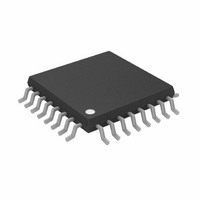
DAC 16BIT DUAL 5V 2LSB 32-TQFP
Manufacturer
Analog Devices Inc
Datasheet
1.AD5763CSUZ.pdf
(28 pages)
Specifications of AD5763CSUZ
Data Interface
Serial
Design Resources
High Accuracy, Bipolar Voltage Output Digital-to-Analog Conversion Using AD5763 (CN0074)
Settling Time
8µs
Number Of Bits
16
Number Of Converters
2
Voltage Supply Source
Dual ±
Power Dissipation (max)
45mW
Operating Temperature
-40°C ~ 105°C
Mounting Type
Surface Mount
Package / Case
32-TQFP, 32-VQFP
Resolution (bits)
16bit
Input Channel Type
Serial
Supply Voltage Range - Analogue
4.75V To 5.25V
Supply Voltage Range - Digital
2.7V To 5.25V
Supply
RoHS Compliant
Lead Free Status / RoHS Status
Lead free / RoHS Compliant
Available stocks
Company
Part Number
Manufacturer
Quantity
Price
Company:

Part Number:
AD5763CSUZ
Manufacturer:
Analog Devices Inc
Quantity:
135
Company:
Part Number:
AD5763CSUZ
Manufacturer:
Analog Devices Inc
Quantity:
10 000
Company:
Part Number:
AD5763CSUZ-REEL7
Manufacturer:
Analog Devices Inc
Quantity:
10 000


AD5763
LAYOUT GUIDELINES
In any circuit where accuracy is important, careful consideration
of the power supply and ground return layout helps to ensure the
rated performance. The printed circuit board (PCB) on which
the AD5763 is mounted should be designed so that the analog
and digital sections are separated and confined to certain areas
of the board. If the AD5763 is in a system where multiple devices
require an AGND-to-DGND connection, the connection should
be made at one point only. Establish the star ground point as
close as possible to the device. The AD5763 should have ample
supply bypassing of 10 μF in parallel with 0.1 μF on each supply
located as close to the package as possible, ideally right up against
the device. The 10 μF capacitors are the tantalum bead type. The
0.1 μF capacitor should have low effective series resistance (ESR)
and low effective series inductance (ESI) such as the common
ceramic types, which provide a low impedance path to ground at
high frequencies to handle transient currents due to internal logic
switching.
The power supply lines of the AD5763 should use as large a
trace as possible to provide low impedance paths and reduce
the effects of glitches on the power supply line. Fast switching
signals, such as clocks, should be shielded with digital ground
to avoid radiating noise to other parts of the board, and should
never be run near the reference inputs. A ground line routed
between the SDIN and SCLK lines helps reduce crosstalk between
them. This is not required on a multilayer board, which has a
separate ground plane, however, it is helpful to separate the
lines. It is essential to minimize noise on the reference inputs,
because it couples through to the DAC output. Avoid crossover
of digital and analog signals. Traces on opposite sides of the
board should run at right angles to each other. This reduces
the effects of feedthrough on the board. A microstrip technique
is recommended, but not always possible with a double-sided
board. In this technique, the component side of the board is
dedicated to ground plane and signal traces are placed on the
solder side.
GALVANICALLY ISOLATED INTERFACE
In many process control applications, it is necessary to provide
an isolation barrier between the controller and the unit being
controlled to protect and isolate the controlling circuitry from
any hazardous common-mode voltages that might occur. Iso-
couplers provide voltage isolation in excess of 2.5 kV. The serial
loading structure of the AD5763 makes it ideal for isolated
Rev. A | Page 26 of 28
interfaces because the number of interface lines is kept to a
minimum. Figure 30 shows a 4-channel isolated interface to
the AD5763 using an ADuM1400.
MICROPROCESSOR INTERFACING
Microprocessor interfacing to the AD5763 is via a serial
bus using a standard protocol that is compatible with micro-
controllers and DSP processors. The communications channel
is a 3-wire minimum interface consisting of a clock signal, a
data signal, and a synchronization signal. The AD5763 requires
a 24-bit data-word with data valid on the falling edge of SCLK.
For all the interfaces, the DAC output update can be done
automatically when all the data is clocked in, or it can be done
under the control of LDAC . The contents of the DAC register
can be read using the readback function.
AD5763 to Blackfin DSP Interface
Figure 31 shows how the AD5763 can be interfaced to an Analog
Devices, Inc., Blackfin® DSP. The Blackfin has an integrated SPI
port that can be connected directly to the SPI pins of the AD5763
and programmable I/O pins that can be used to set the state of a
digital input such as the LDAC pin.
1
ADDITIONAL PINS OMITTED FOR CLARITY.
CONTROLLER
SERIAL CLOCK
CONTROL OUT
SERIAL DATA
MICRO-
SYNC OUT
OUT
OUT
ADSP-BF531
SPISELx
V
V
V
V
Figure 31. AD5763 to Blackfin Interface
ADuM1400
IA
IB
IC
ID
MOSI
PF10
SCK
Figure 30. Isolated Interface
ENCODE
ENCODE
ENCODE
ENCODE
1
DECODE
DECODE
DECODE
DECODE
SYNC
SCLK
SDIN
LDAC
AD5763
V
V
V
V
OA
OB
OC
OD
TO SCLK
TO SDIN
TO SYNC
TO LDAC
Related parts for AD5763CSUZ
Image
Part Number
Description
Manufacturer
Datasheet
Request
R

Part Number:
Description:
±1.7g Dual-Axis IMEMS Accelerometer Evaluation Board
Manufacturer:
Analog Devices Inc
Datasheet:

Part Number:
Description:
Inertial Sensor Evaluation System
Manufacturer:
Analog Devices Inc
Datasheet:
Part Number:
Description:
Manufacturer:
Analog Devices Inc
Datasheet:
Part Number:
Description:
Manufacturer:
Analog Devices Inc
Datasheet:
Part Number:
Description:
Manufacturer:
Analog Devices Inc
Datasheet:
Part Number:
Description:
Manufacturer:
Analog Devices Inc
Datasheet:
Part Number:
Description:
Manufacturer:
Analog Devices Inc
Datasheet:
Part Number:
Description:
Manufacturer:
Analog Devices Inc
Datasheet:
Part Number:
Description:
Manufacturer:
Analog Devices Inc
Datasheet:
Part Number:
Description:
Manufacturer:
Analog Devices Inc
Datasheet:
Part Number:
Description:
Manufacturer:
Analog Devices Inc
Datasheet:
Part Number:
Description:
Manufacturer:
Analog Devices Inc
Datasheet:
Part Number:
Description:
Manufacturer:
Analog Devices Inc
Datasheet: