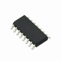
CS4341A-KSZ Cirrus Logic Inc, CS4341A-KSZ Datasheet - Page 14

CS4341A-KSZ
Manufacturer Part Number
CS4341A-KSZ
Description
IC DAC STER 24BIT 192KHZ 16SOIC
Manufacturer
Cirrus Logic Inc
Datasheet
1.CS4341A-KSZ.pdf
(34 pages)
Specifications of CS4341A-KSZ
Package / Case
16-SOIC
Number Of Bits
24
Data Interface
Serial
Number Of Converters
2
Voltage Supply Source
Single Supply
Power Dissipation (max)
90mW
Operating Temperature
-10°C ~ 70°C
Mounting Type
Surface Mount
Conversion Rate
192 KSPS
Resolution
24 bit
Interface Type
Serial
Operating Supply Voltage
3.3 V or 5 V
Operating Temperature Range
+ 70 C
Maximum Power Dissipation
125 mW
Mounting Style
SMD/SMT
Number Of Dac Outputs
2
Lead Free Status / RoHS Status
Lead free / RoHS Compliant
Settling Time
-
Lead Free Status / Rohs Status
Lead free / RoHS Compliant
Other names
598-1633
Available stocks
Company
Part Number
Manufacturer
Quantity
Price
Company:
Part Number:
CS4341A-KSZ
Manufacturer:
CIRRUS
Quantity:
676
Part Number:
CS4341A-KSZ
Manufacturer:
CIRRUS
Quantity:
20 000
14
3.9.4
In SPI mode, data is clocked into the serial control data line, CDIN, by the serial control port clock,
CCLK (see Figure 7 for the clock to data relationship). There is no AD0 pin. Pin CS is the chip
select signal and is used to control SPI writes to the control port. When the device detects a high to
low transition on the AD0/CS pin after power-up, SPI mode will be selected. All signals are inputs
and data is clocked in on the rising edge of CCLK.
3.9.4a
To write to the device, follow the procedure below while adhering to the control port
Switching Specifications in section 6.
1) Bring CS low.
2) The address byte on the CDIN pin must then be 00100000.
3) Write to the memory address pointer, MAP. This byte points to the register to be written.
4) Write the desired data to the register pointed to by the MAP.
5) If the INCR bit (see section 3.9.2) is set to 1, repeat the previous step until all the desired
registers are written, then bring CS high.
6) If the INCR bit is set to 0 and further SPI writes to other registers are desired, it is nec-
essary to bring CS high, and follow the procedure detailed from step 1. If no further writes
to other registers are desired, bring CS high.
SPI Mode
SPI Write
CS
C C L K
C D IN
Figure 7. Control Port Timing, SPI mode
M A P = M em ory A d dress P oin te r
ADDRESS
0 0 1 0 0 0 0
C H IP
R/W
M A P
MSB
byte 1
DATA
byte n
L S B
CS4341A
DS582F2


