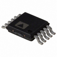
AD5446YRMZ Analog Devices Inc, AD5446YRMZ Datasheet - Page 23

AD5446YRMZ
Manufacturer Part Number
AD5446YRMZ
Description
IC DAC 14BIT MULTIPLYING 10-MSOP
Manufacturer
Analog Devices Inc
Datasheet
1.AD5446YRMZ.pdf
(28 pages)
Specifications of AD5446YRMZ
Data Interface
DSP, MICROWIRE™, QSPI™, Serial, SPI™
Design Resources
Versatile High Precision Programmable Current Sources Using DACs, Op Amps, and MOSFET Transistors (CN0151)
Number Of Bits
14
Number Of Converters
1
Voltage Supply Source
Single Supply
Power Dissipation (max)
50.5µW
Operating Temperature
-40°C ~ 125°C
Mounting Type
Surface Mount
Package / Case
10-MSOP, Micro10™, 10-uMAX, 10-uSOP
Resolution (bits)
14bit
Sampling Rate
2.7MSPS
Input Channel Type
Serial
Supply Voltage Range - Analog
2.5V To 5.5V
Supply Current
400nA
Digital Ic Case Style
SOP
Lead Free Status / RoHS Status
Lead free / RoHS Compliant
For Use With
EVAL-AD5446EBZ - BOARD EVALUATION FOR AD5446
Settling Time
-
Lead Free Status / RoHS Status
Lead free / RoHS Compliant, Lead free / RoHS Compliant
Available stocks
Company
Part Number
Manufacturer
Quantity
Price
Company:
Part Number:
AD5446YRMZ
Manufacturer:
ADI
Quantity:
352
Part Number:
AD5446YRMZ
Manufacturer:
ADI/亚德诺
Quantity:
20 000
PCB LAYOUT AND POWER SUPPLY DECOUPLING
In any circuit where accuracy is important, careful considera-
tion of the power supply and ground return layout helps to
ensure the rated performance. The printed circuit boards on
which the AD5444/AD5446 are mounted should be designed
so the analog and digital sections are separated and confined to
certain areas of the board. If the DACs are in systems in which
multiple devices require a AGND-to-DGND connection, the
connection should be made at one point only. The star ground
point should be established as close as possible to the devices.
The DAC should have ample supply bypassing of 10 μF in
parallel with 0.1 μF on the supply located as close to the pack-
age as possible, ideally right up against the device. The 0.1 μF
capacitor should have low effective series resistance (ESR)
and effective series inductance (ESI), like the common ceramic
types that provide a low impedance path to ground at high
frequencies, to handle transient currents due to internal logic
switching. Low ESR, 1 μF to 10 μF tantalum or electrolytic
capacitors should also be applied at the supplies to minimize
transient disturbance and filter out low frequency ripple.
Fast switching signals such as clocks should be shielded with
digital ground to avoid radiating noise to other parts of the
board, and should never be run near the reference inputs.
Avoid crossover of digital and analog signals. Traces on oppo-
site sides of the board should run at right angles to each other.
This reduces the effects of feedthrough throughout the board.
Rev. C | Page 23 of 28
A microstrip technique, by far the best, is not always possible
with a double-sided board. In this technique, the component
side of the board is dedicated to the ground plane, while signal
traces are placed on the solder side.
It is good practice to employ compact, minimum lead-length
PCB layout design. Leads to the input should be as short as
possible to minimize IR drops and stray inductance.
The PCB metal traces between V
matched to minimize gain error. To maximize high frequency
performance, the I-to-V amplifier should be located as close
to the device as possible.
EVALUATION BOARD FOR THE DAC
The evaluation board consists of an AD5444 or AD5446 DAC
and a current-to-voltage amplifier, AD8065. Included on the
evaluation board is a 10 V reference, ADR01. An external
reference can also be applied via an SMB input.
The evaluation kit consists of a CD with self-installing PC
software to control the DAC. The software allows the user
to write a code to the device.
POWER SUPPLIES FOR THE EVALUATION BOARD
The board requires ±12 V and +5 V supplies. The ±12 V V
and V
supply is used to power the DAC (V
Both supplies are decoupled to their respective ground plane
with 10 μF tantalum and 0.1 μF ceramic capacitors.
SS
are used to power the output amplifier, while the +5 V
REF
and R
DD1
AD5444/AD5446
) and transceivers (V
FB
should also be
DD
CC
).


