MCP4728-E/UN Microchip Technology, MCP4728-E/UN Datasheet - Page 43
MCP4728-E/UN
Manufacturer Part Number
MCP4728-E/UN
Description
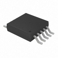
IC DAC 12BIT W/I2C 10-MSOP
Manufacturer
Microchip Technology
Specifications of MCP4728-E/UN
Number Of Converters
4
Settling Time
6µs
Package / Case
10-MSOP, Micro10™, 10-uMAX, 10-uSOP
Number Of Bits
12
Data Interface
I²C
Voltage Supply Source
Single Supply
Operating Temperature
-40°C ~ 125°C
Mounting Type
Surface Mount
Number Of Dac Outputs
4
Resolution
12 bit
Interface Type
I2C
Supply Voltage (max)
5.5 V
Supply Voltage (min)
2.7 V
Maximum Operating Temperature
+ 125 C
Mounting Style
SMD/SMT
Minimum Operating Temperature
- 40 C
Supply Current
110 mA
Voltage Reference
2.048 V
Lead Free Status / RoHS Status
Lead free / RoHS Compliant
For Use With
MCP4728EV - BOARD EVAL 12BIT 4CH DAC MCP4728
Power Dissipation (max)
-
Lead Free Status / Rohs Status
Lead free / RoHS Compliant
Available stocks
Company
Part Number
Manufacturer
Quantity
Price

Part Number:
MCP4728-E/UN
Manufacturer:
MICROCHIP/微芯
Quantity:
20 000


FIGURE 5-12:
Registers.
FIGURE 5-13:
Registers.
© 2009 Microchip Technology Inc.
Command Type Bits:
Command Type Bits:
Start
S
(C2 C1 C0)
1
1
Command
1
Write
Start
0
Device Addressing
S
0
1
Note 1: V
Note 1:
1
1st byte
0 A2 A1 A0
X
Device Addressing
1
2:
Write Command: Write Voltage Reference Selection Bit (V
Write Command: Write Power-Down Selection Bits (PD1, PD0) to the DAC Input
PD1 A PD0 A PD1 B PD0 B A
Channel A
0
V
V
V
V
X is don’t care bit.
X is don’t care bit.
REF
REF
REF
REF
REF
C2=1
C2=1
1st byte
0
= 1: Internal Reference (2.048V)
= 0: V
A = Voltage reference of Channel A
B = Voltage reference of Channel B
C = Voltage reference of Channel C
D = Voltage reference of Channel D
ACK (MCP4728)
A2 A1 A0
R/W
2nd Byte
0
DD
C1=0
C1=0
A
Channel B
R/W
0
C0=0
C0=1
A
(C2 C1 C0)
1
Command
Write
PD1 C PD0 C PD1 D
0
Channel C
0
X V
ACK (MCP4728)
Registers and V
at this falling edge of ACK pulse.
REF
ACK (MCP4728)
A V
at this falling edge of ACK pulse.
Registers and V
Channel D
2nd Byte
REF
3rd Byte
Note 1
PD0 D
B V
OUT
REF
are updated
REF
OUT
C V
X
) to the DAC Input
are updated
REF
MCP4728
X
D A
X
DS22187A-page 43
X
Stop
P
A
Stop
P
Related parts for MCP4728-E/UN
Image
Part Number
Description
Manufacturer
Datasheet
Request
R

Part Number:
Description:
12-bit, Quad Digital-to-analog Converter With Eeprom Memory
Manufacturer:
Microchip Technology Inc.
Datasheet:
Part Number:
Description:
Manufacturer:
Microchip Technology Inc.
Datasheet:
Part Number:
Description:
Manufacturer:
Microchip Technology Inc.
Datasheet:
Part Number:
Description:
Manufacturer:
Microchip Technology Inc.
Datasheet:
Part Number:
Description:
Manufacturer:
Microchip Technology Inc.
Datasheet:
Part Number:
Description:
Manufacturer:
Microchip Technology Inc.
Datasheet:
Part Number:
Description:
Manufacturer:
Microchip Technology Inc.
Datasheet:
Part Number:
Description:
Manufacturer:
Microchip Technology Inc.
Datasheet:
Part Number:
Description:
Manufacturer:
Microchip Technology Inc.
Datasheet: