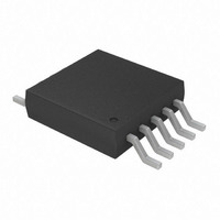
MCP4728-E/UN Microchip Technology, MCP4728-E/UN Datasheet - Page 23

MCP4728-E/UN
Manufacturer Part Number
MCP4728-E/UN
Description
IC DAC 12BIT W/I2C 10-MSOP
Manufacturer
Microchip Technology
Specifications of MCP4728-E/UN
Number Of Converters
4
Settling Time
6µs
Package / Case
10-MSOP, Micro10™, 10-uMAX, 10-uSOP
Number Of Bits
12
Data Interface
I²C
Voltage Supply Source
Single Supply
Operating Temperature
-40°C ~ 125°C
Mounting Type
Surface Mount
Number Of Dac Outputs
4
Resolution
12 bit
Interface Type
I2C
Supply Voltage (max)
5.5 V
Supply Voltage (min)
2.7 V
Maximum Operating Temperature
+ 125 C
Mounting Style
SMD/SMT
Minimum Operating Temperature
- 40 C
Supply Current
110 mA
Voltage Reference
2.048 V
Lead Free Status / RoHS Status
Lead free / RoHS Compliant
For Use With
MCP4728EV - BOARD EVAL 12BIT 4CH DAC MCP4728
Power Dissipation (max)
-
Lead Free Status / Rohs Status
Lead free / RoHS Compliant
Available stocks
Company
Part Number
Manufacturer
Quantity
Price
Part Number:
MCP4728-E/UN
Manufacturer:
MICROCHIP/微芯
Quantity:
20 000
4.0
The MCP4728 device is a 12-bit 4-channel buffered
voltage
(EEPROM). The user can program the EEPROM with
I
each channel. The device has an internal charge pump
circuit to provide the programming voltage of the
EEPROM.
When the device is first powered-up, it automatically
loads the stored data in its EEPROM to the DAC input
and output registers, and provides analog outputs with
the saved settings immediately. This event does not
require LDAC or UDAC bit condition. After the device is
powered-up, the user can update the input registers
using I
updated with new register values if LDAC pin or UDAC
bit is low. The DAC output of each channel is buffered
with a low power and precision output amplifier. This
amplifier provides a rail-to-rail output with low offset
voltage and low noise.
The device uses a resistor string architecture. The
resistor ladder DAC can be driven from V
V
can select internal (2.048V) or external reference (V
for each DAC channel individually by software control.
The V
channel is controlled and operated independently.
The device has a Power-Down mode feature. Most of
the circuit in each
off. Therefore, operating power can be saved
significantly by putting any unused channel to the
Power-Down mode.
4.1
The device contains an internal Power-On-Reset
(POR) circuit that monitors power supply voltage (V
during operation. This circuit ensures correct device
start-up at system power-up and power-down events.
If the power supply voltage is less than the POR
threshold (V
and there will be no analog output. When the V
increases above the V
state. During the reset period, each channel uploads all
configuration and DAC input codes from EEPROM,
and analog output (V
This enables the device to return to the same state that
it was at the last write to the EEPROM before it was
powered off. The POR status is monitored by the POR
status bit by using the I
Figure 5-15
The POR circuit is also powered off if all channels are
powered down during the Power-Down mode.
© 2009 Microchip Technology Inc.
2
REF
C address bits, configuration and DAC input data of
depending on the reference selection. The user
2
DD
C write commands. The analog outputs can be
THEORY OF DEVICE
OPERATION
Power-On-Reset (POR)
output
is used as the external reference. Each
for the details of the POR status bit.
POR
= 2V, typical), all circuits are disabled
DAC
powered down
OUT
POR
) will be available accordingly.
with
, the device takes a reset
2
C read command. See
non-volatile
channel are turned
DD
or internal
memory
DD
DD
DD
)
)
4.2
The device can be reset by two independent events: (a)
by Power-On-Reset or (b) by I
Command. Under the reset conditions, the device
uploads the EEPROM data into both of the DAC input
and output registers simultaneously. The analog output
voltage of each channel is available immediately
regardless of the LDAC and UDAC bit conditions.
The factory default settings for the EEPROM prior to
the device shipment are shown in
4.3
The DAC output is buffered with a low power precision
amplifier. This amplifier provides low offset voltage and
low noise, as well as rail-to-rail output.
The output amplifier can drive the resistive and high
capacitive loads without oscillation. The amplifier can
provide a maximum load current of 24 mA which is
enough for most of programmable voltage reference
applications.
Characteristics” for the specifications of the output
amplifier.
4.3.1
The rail-to-rail output amplifier of each channel has
configurable gain option. When the internal voltage
reference is selected, the output amplifier gain has two
selection options: gain of 1 or gain of 2.
When the external reference is selected (V
the gain of 2 option is disabled, and only the gain of 1
is used by default.
4.3.1.1
The analog output (V
capacitive loads up to 1000 pF in parallel with 5 kΩ
load resistance.
Resistive Load.
Reset Conditions
Output Amplifier
PROGRAMMABLE GAIN BLOCK
Resistive and Capacitive Loads
Refer
Figure 2-42
OUT
to
) pin is capable of driving
Section 1.0
MCP4728
2
shows the V
C General Call Reset
Table
DS22187A-page 23
4-2.
REF
“Electrical
OUT
= V
DD
vs.
),


