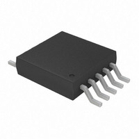
MCP4728-E/UN Microchip Technology, MCP4728-E/UN Datasheet - Page 4

MCP4728-E/UN
Manufacturer Part Number
MCP4728-E/UN
Description
IC DAC 12BIT W/I2C 10-MSOP
Manufacturer
Microchip Technology
Specifications of MCP4728-E/UN
Number Of Converters
4
Settling Time
6µs
Package / Case
10-MSOP, Micro10™, 10-uMAX, 10-uSOP
Number Of Bits
12
Data Interface
I²C
Voltage Supply Source
Single Supply
Operating Temperature
-40°C ~ 125°C
Mounting Type
Surface Mount
Number Of Dac Outputs
4
Resolution
12 bit
Interface Type
I2C
Supply Voltage (max)
5.5 V
Supply Voltage (min)
2.7 V
Maximum Operating Temperature
+ 125 C
Mounting Style
SMD/SMT
Minimum Operating Temperature
- 40 C
Supply Current
110 mA
Voltage Reference
2.048 V
Lead Free Status / RoHS Status
Lead free / RoHS Compliant
For Use With
MCP4728EV - BOARD EVAL 12BIT 4CH DAC MCP4728
Power Dissipation (max)
-
Lead Free Status / Rohs Status
Lead free / RoHS Compliant
Available stocks
Company
Part Number
Manufacturer
Quantity
Price
Part Number:
MCP4728-E/UN
Manufacturer:
MICROCHIP/微芯
Quantity:
20 000
MCP4728
TABLE 1-1:
DS22187A-page 4
Electrical Specifications: Unless otherwise indicated, all parameters apply at V
R
Power-On-Reset
Threshold Voltage
Power-Up Ramp Rate
DC Accuracy
Resolution
INL Error
DNL Error
Offset Error
Offset Error Drift
Gain Error
Gain Error Drift
Internal Voltage Reference (V
Internal Voltage Reference
Temperature Coefficient
Reference Output Noise
Output Noise Density
1/f Corner Frequency
Analog Output (Output Amplifier)
Output Voltage Swing
Note 1:
L
= 5 kΩ, C
2:
3:
4:
5:
6:
7:
8:
9:
Parameter
All digital input pins (SDA, SCL, LDAC) are tied to “High”, Output pins are unloaded, code = 0x000.
The power-up ramp rate measures the rise of V
This parameter is ensured by design and not 100% tested.
This parameter is ensured by characterization and not 100% tested.
Test code range: 100 - 4000 codes, V
Time delay to settle to a new reference when switching from external to internal reference or vice versa.
This parameter is indirectly tested by Offset and Gain error testing.
Within 1/2 LSB of the final value when code changes from 1/4 of to 3/4 of full scale.
This time delay is measured from the falling edge of ACK pulse in I
This time delay is not included in the output settling time specification.
L
= 100 pF, G
ELECTRICAL CHARACTERISTICS (CONTINUED)
X
= 1, T
ΔV
ΔV
f
Symbol
ΔG
CORNER
V
E
e
V
V
V
REF
DNL
V
RAMP
REF
INL
NREF
NREF
OS
G
POR
REF
OUT
n
OS
E
A
E
/°C
/°C
), (Note 3)
= -40°C to +125°C. Typical values are at +25°C, V
/°C
2.007
-0.75
Min
12
—
—
—
—
—
—
—
—
—
—
—
—
—
—
—
-3
-3
-2
1
REF
Typical
±0.16
2.048
±0.44
FSR
±0.2
0.02
0.25
0.09
= V
-0.1
-0.1
-0.1
125
290
400
2.2
1.2
1.0
—
±2
45
—
-3
DD
DD
, V
DD
over time.
±0.75
2.089
Max
0.75
±13
—
—
—
—
—
—
—
—
—
—
—
—
—
—
—
3
3
2
= 5.5V.
ppm/°C
LSB/°C
ppm/°C
ppm/°C -45°C to 25°C
ppm/°C +25°C to +125°C
ppm/°C
LSB/°C
µV
μV
Units
% of
FSR
% of
FSR
% of
FSR
% of
FSR
Hz
LSB
LSB
Bits
V/s
V
V
p-p
V
H
2
Z
C command to the beginning of V
DD
All circuits including EEPROM are
ready to operate.
Note 2, Note 4
Code Change: 000h to FFFh
(Note 5)
(Note 5)
Code = 000h
V
Code = FFFh,
Offset error is not included.
V
Code = FFFh,
Offset error is not included.
V
Code = FFFh,
Offset error is not included.
-40 to 0°C
-40 to 0°C
0 to +125°C
0 to +125°C
Code = FFFh,
0.1 - 10 Hz, G
Code = FFFh, 1 kHz, G
Code = FFFh, 10 kHz, G
(Note 7)
REF
REF
REF
= + 2.7V to 5.5V, V
IH
© 2009 Microchip Technology Inc.
= Internal, Gain = x1
= Internal, Gain = x2
= V
= V
DD
DD
Conditions
, V
x
=1
IL
= V
SS.
SS
x
= 0V,
=1
x
=1
OUT
.


