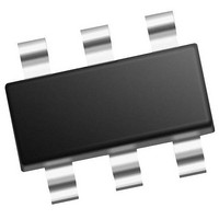
PIC10F322T-I/OT Microchip Technology, PIC10F322T-I/OT Datasheet - Page 119

PIC10F322T-I/OT
Manufacturer Part Number
PIC10F322T-I/OT
Description
896 B Flash, 64 B RAM, 4 I/O, 8bit ADC, PWM, CLC, DDS, CWG, TEMP Indicator, 2.3V
Manufacturer
Microchip Technology
Datasheet
1.PIC10F320-IOT.pdf
(210 pages)
Specifications of PIC10F322T-I/OT
Core
RISC
Processor Series
PIC10F
Data Bus Width
8 bit
Maximum Clock Frequency
31 KHz
Program Memory Size
512 B
Data Ram Size
64 B
Number Of Programmable I/os
4
Number Of Timers
2
Operating Temperature Range
- 40 C to + 85 C
Package / Case
SOT-23-6
Mounting Style
SMD/SMT
Maximum Operating Temperature
+ 85 C
Program Memory Type
Flash
Lead Free Status / Rohs Status
Details
Available stocks
Company
Part Number
Manufacturer
Quantity
Price
Company:
Part Number:
PIC10F322T-I/OT
Manufacturer:
VISHAY
Quantity:
11 490
Part Number:
PIC10F322T-I/OT
Manufacturer:
MICROCHIP/微芯
Quantity:
20 000
- Current page: 119 of 210
- Download datasheet (2Mb)
19.5
REGISTER 19-1:
2011 Microchip Technology Inc.
bit 7
Legend:
R = Readable bit
u = Bit is unchanged
‘1’ = Bit is set
bit 7
bit 6
bit 5
bit 4
bit 3
bit 2-0
R/W-0/0
LCxEN
CLC Control Registers
LCxEN: Configurable Logic Cell Enable bit
1 = Configurable Logic Cell is enabled and mixing input signals
0 = Configurable Logic Cell is disabled and has logic zero output
LCxOE: Configurable Logic Cell Output Enable bit
1 = Configurable Logic Cell port pin output enabled
0 = Configurable Logic Cell port pin output disabled
LCxOUT: Configurable Logic Cell Data Output bit
Read-only: logic cell output data, after LCxPOL; sampled from lcx_out wire.
LCxINTP: Configurable Logic Cell Positive Edge Going Interrupt Enable bit
1 = CLCxIF will be set when a rising edge occurs on lcx_out
0 = CLCxIF will not be set
LCxINTN: Configurable Logic Cell Negative Edge Going Interrupt Enable bit
1 = CLCxIF will be set when a falling edge occurs on lcx_out
0 = CLCxIF will not be set
LCxMODE<2:0>: Configurable Logic Cell Functional Mode bits
111 = Cell is 1-input transparent latch with S and R
110 = Cell is J-K Flip-Flop with R
101 = Cell is 2-input D Flip-Flop with R
100 = Cell is 1-input D Flip-Flop with S and R
011 = Cell is S-R latch
010 = Cell is 4-input AND
001 = Cell is OR-XOR
000 = Cell is AND-OR
R/W-0/0
LCxOE
CLCxCON: CONFIGURABLE LOGIC CELL CONTROL REGISTER
W = Writable bit
x = Bit is unknown
‘0’ = Bit is cleared
LCxOUT
R-0/0
LCxINTP
R/W-0/0
Preliminary
U = Unimplemented bit, read as ‘0’
-n/n = Value at POR and BOR/Value at all other Reset
LCxINTN
R/W-0/0
PIC10(L)F320/322
R/W-0/0
LCxMODE<2:0>
R/W-0/0
DS41585A-page 119
R/W-0/0
bit 0
Related parts for PIC10F322T-I/OT
Image
Part Number
Description
Manufacturer
Datasheet
Request
R

Part Number:
Description:
896 B Flash, 64 B RAM, 4 I/O, 8bit ADC, PWM, CLC, DDS, CWG, TEMP Indicator, 2.3V
Manufacturer:
Microchip Technology

Part Number:
Description:
896 B Flash, 64 B RAM, 4 I/O, 8bit ADC, PWM, CLC, DDS, CWG, TEMP Indicator, 2.3V
Manufacturer:
Microchip Technology

Part Number:
Description:
896 B Flash, 64 B RAM, 4 I/O, 8bit ADC, PWM, CLC, DDS, CWG, TEMP Indicator, 2.3V
Manufacturer:
Microchip Technology

Part Number:
Description:
896 B Flash, 64 B RAM, 4 I/O, 8bit ADC, PWM, CLC, DDS, CWG, TEMP Indicator, 2.3V
Manufacturer:
Microchip Technology

Part Number:
Description:
896 B Flash, 64 B RAM, 4 I/O, 8bit ADC, PWM, CLC, DDS, CWG, TEMP Indicator, 2.3V
Manufacturer:
Microchip Technology

Part Number:
Description:
896 B Flash, 64 B RAM, 4 I/O, 8bit ADC, PWM, CLC, DDS, CWG, TEMP Indicator, 2.3V
Manufacturer:
Microchip Technology

Part Number:
Description:
384B Flash, 16B RAM, 4 I/O, 8bit ADC 6 SOT-23 BAG
Manufacturer:
Microchip Technology
Datasheet:

Part Number:
Description:
768B Flash, 23B RAM, 4 I/O, 8bit ADC 6 SOT-23 BAG
Manufacturer:
Microchip Technology
Datasheet:

Part Number:
Description:
384B Flash, 16B RAM, 4 I/O, 8bit ADC 6 SOT-23 BAG
Manufacturer:
Microchip Technology
Datasheet:

Part Number:
Description:
768B Flash, 23B RAM, 4 I/O, 8bit ADC 6 SOT-23 BAG
Manufacturer:
Microchip Technology
Datasheet:

Part Number:
Description:
PIC10F PROGRAMMER ADAPTER (SOT-23), PICKIT
Manufacturer:
Microchip Technology Inc.

Part Number:
Description:
Manufacturer:
Microchip Technology Inc.
Datasheet:

Part Number:
Description:
Manufacturer:
Microchip Technology Inc.
Datasheet:


