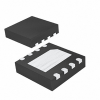
MAX5432LETA+T Maxim Integrated Products, MAX5432LETA+T Datasheet - Page 4

MAX5432LETA+T
Manufacturer Part Number
MAX5432LETA+T
Description
IC POT DGTL 32-TAP NV I2C 8-TDFN
Manufacturer
Maxim Integrated Products
Datasheet
1.MAX5434LEZTT.pdf
(19 pages)
Specifications of MAX5432LETA+T
Taps
32
Resistance (ohms)
50K
Number Of Circuits
1
Temperature Coefficient
35 ppm/°C Typical
Memory Type
Non-Volatile
Interface
I²C, 2-Wire Serial
Voltage - Supply
2.7 V ~ 5.25 V
Operating Temperature
-40°C ~ 85°C
Mounting Type
Surface Mount
Package / Case
8-TDFN Exposed Pad
Resistance In Ohms
50K
Number Of Pots
Single
Taps Per Pot
32
Resistance
50 KOhms
Wiper Memory
Non Volatile
Digital Interface
Serial (2-Wire, I2C)
Operating Supply Voltage
5 V
Supply Current
0.002 mA
Maximum Operating Temperature
+ 85 C
Minimum Operating Temperature
- 40 C
Description/function
32-Tap, Nonvolatile, I2C, Linear, Digital Potentiometers, 50kohm Resistor Divider
Mounting Style
SMD/SMT
Supply Voltage (max)
5.25 V
Supply Voltage (min)
2.7 V
Tolerance
25 %
Lead Free Status / RoHS Status
Lead free / RoHS Compliant
Other names
MAX5432LETA+T
32-Tap, Nonvolatile, I
Potentiometers
TIMING CHARACTERISTICS (continued)
(V
+25°C.) (Figures 1 and 2) (Note 1)
4
Note 2: The DNL and INL are measured with the potentiometer configured as a variable resistor. For the 3-terminal potentiometers
Note 3: The DNL and INL are measured with the potentiometer configured as a voltage-divider with H = V
Note 4: Full-scale error is defined as
Note 5: Zero-scale error is defined as
Note 6: The wiper resistance is the worst value measured by injecting the currents given in Note 2 into W with L = GND.
Note 7: The device draws current in excess of the specified supply current when the digital inputs are driven with voltages between
Note 8: Wiper is at midscale with a 10pF capacitive load. Potentiometer set to midscale, L = GND, an AC source is applied to H,
Note 9: This is measured from the STOP pulse to the time it takes the output to reach 50% of the output step size (divider mode). It
Note 10: The programming current exists only during NV writes (12ms typ).
Note 11: Digital timing is guaranteed by design and characterization, and is not production tested.
Note 12: An appropriate bus pullup resistance must be selected depending on board capacitance. Refer to the I
Note 13: The idle time begins from the initiation of the stop pulse.
(V
DD
DD
1.5
1.2
0.9
0.6
0.3
_______________________________________________________________________________________
0
= +2.7V to +5.25V, V
= +5V, T
-40
(MAX5432/MAX5433), H is unconnected and L = GND. At V
configuration, and 40µA for the 100kΩ configuration. At V
configuration, and 20µA for the 100kΩ configuration.
(MAX5432/MAX5433 only). The wiper terminal is unloaded and measured with an ideal voltmeter.
DIGITAL INPUTS = GND OR V
R
(V
and the output is measured as 3dB lower than the DC W/H value in dB.
is measured with a maximum external capacitive load of 10pF.
tion document linked to this web address: www.semiconductors.philips.com/acrobat/literature/9398/39340011.pdf
W
DD
V
STANDBY SUPPLY CURRENT
DD
= (V
-15
A
= 3V
- 0.5V) and (GND + 0.5V). See the Supply Current vs. Digital Input Voltage graph in the Typical Operating Characteristics.
= +25°C, unless otherwise noted.)
vs. TEMPERATURE
W
TEMPERATURE (°C)
- V
10
H
) / I
35
H
W
V
DD
DD
= V
.
= 5V
DD
60
, V
L
= GND, T
85
V
V
⎛
⎜
⎝
W
⎛
⎜
⎝
W
V
31
V
31
H
-
H
-
V
⎞
⎟
⎠
V
H
⎞
⎟
⎠
L
.
.
1.0
0.8
0.6
0.4
0.2
A
0
= -40°C to +85°C, unless otherwise noted. Typical values are at V
2.5
DIGITAL INPUTS = GND OR V
3.0
2
vs. SUPPLY VOLTAGE
SUPPLY CURRENT
SUPPLY VOLTAGE (V)
C, Linear, Digital
3.5
DD
4.0
DD
= 3V, W is driven with a source current of 40µA for the 50kΩ
Typical Operating Characteristics
= 5V, W is driven with a source current of 80µA for the 50kΩ
DD
4.5
5.0
5.5
1000
100
0.1
10
1
0
vs. DIGITAL INPUT VOLTAGE
1
DIGITAL INPUT VOLTAGE (V)
DD
SUPPLY CURRENT
and L = GND
2
2
C-bus specifica-
V
DD
V
3
DD
DD
= 3V
= 5V
= +5V, T
4
A
5
=


