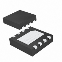
MAX5432LETA+T Maxim Integrated Products, MAX5432LETA+T Datasheet - Page 10

MAX5432LETA+T
Manufacturer Part Number
MAX5432LETA+T
Description
IC POT DGTL 32-TAP NV I2C 8-TDFN
Manufacturer
Maxim Integrated Products
Datasheet
1.MAX5434LEZTT.pdf
(19 pages)
Specifications of MAX5432LETA+T
Taps
32
Resistance (ohms)
50K
Number Of Circuits
1
Temperature Coefficient
35 ppm/°C Typical
Memory Type
Non-Volatile
Interface
I²C, 2-Wire Serial
Voltage - Supply
2.7 V ~ 5.25 V
Operating Temperature
-40°C ~ 85°C
Mounting Type
Surface Mount
Package / Case
8-TDFN Exposed Pad
Resistance In Ohms
50K
Number Of Pots
Single
Taps Per Pot
32
Resistance
50 KOhms
Wiper Memory
Non Volatile
Digital Interface
Serial (2-Wire, I2C)
Operating Supply Voltage
5 V
Supply Current
0.002 mA
Maximum Operating Temperature
+ 85 C
Minimum Operating Temperature
- 40 C
Description/function
32-Tap, Nonvolatile, I2C, Linear, Digital Potentiometers, 50kohm Resistor Divider
Mounting Style
SMD/SMT
Supply Voltage (max)
5.25 V
Supply Voltage (min)
2.7 V
Tolerance
25 %
Lead Free Status / RoHS Status
Lead free / RoHS Compliant
Other names
MAX5432LETA+T
32-Tap, Nonvolatile, I
Potentiometers
X = Don’t care.
Figure 2. Load Circuit
Figure 4. Slave Address
Use the command byte to select the destination of the
wiper data (nonvolatile or volatile memory registers)
and swap data between nonvolatile and volatile memo-
ry registers (see Table 2).
The MAX5432–MAX5435 use the first 5 bits (MSBs,
D7–D3) of the data byte to set the position of the wiper.
The last 3 bits (D2, D1, and D0) are don’t care bits (see
Table 2).
Table 2. Command Byte Summary
10
NVREGxVREG
VREGxNVREG
SCL CYCLE
NUMBER
NVREG
REGISTER
VREG
______________________________________________________________________________________
SDA
SCL
*SEE THE Ordering Information/Selector Guide FOR OTHER ADDRESS OPTIONS.
MSB
0
SDA
A6 A5 A4 A3 A2 A1 A0
1
0
0
0
0
2
1
1
1
1
ADDRESS BYTE
1
3
0
0
0
0
V
DD
4
1
1
1
1
I
I
OL
OH
A2 A1 A0
A2 A1 A0
A2 A1 A0
A2 A1 A0
= 3mA
5
= 0mA
6
400pF
0
V
OUT
7
Command Byte
P/
W
N
O
8
0
0
0
0
Data Byte
C
9
A
K
1
10 11 12 13 14 15 16 17 18 19 20 21 22 23 24 25 26 27
C7 C6 C5 C4 C3 C2 C1 C0
0
0
0
0
2
0
0
1
1
C, Linear, Digital
COMMAND BTYE
0
1
1
0
0*
1
0
0
1
VREG: The data byte writes to the volatile memory reg-
ister and the wiper position updates with the data in the
volatile memory register.
NVREG: The data byte writes to the nonvolatile memory
register. The wiper position is unchanged.
NVREGxVREG: Data transfers from the nonvolatile
memory register to the volatile memory register (wiper
position updates).
VREGxNVREG: Data transfers from the volatile memory
register into the nonvolatile memory register.
Figure 3. Start and Stop Conditions
SDA
SCL
CONDITION
0
0
0
0
START
S
0
0
0
0
0*
0
0
0
0
1
1
1
1
C
A
K
LSB
A0
D7 D6 D5 D4 D3 D2 D1 D0
D7 D6 D5 D4 D3
D7 D6 D5 D4 D3
D7 D6 D5 D4 D3
D7 D6 D5 D4 D3
DATA BYTE
NOP/W
Command Descriptions
X
X
X
X
ACK
X
X
X
X
X
X
X
X
CONDITION
STOP
C
A
K
P


