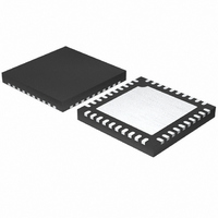
MAX1359BETL+ Maxim Integrated Products, MAX1359BETL+ Datasheet - Page 62

MAX1359BETL+
Manufacturer Part Number
MAX1359BETL+
Description
IC DAS 16BIT 40-TQFN
Manufacturer
Maxim Integrated Products
Type
Data Acquisition System (DAS)r
Specifications of MAX1359BETL+
Resolution (bits)
16 b
Sampling Rate (per Second)
21.84k
Data Interface
Serial
Voltage Supply Source
Analog and Digital
Voltage - Supply
1.8 V ~ 3.6 V
Operating Temperature
-40°C ~ 85°C
Mounting Type
Surface Mount
Package / Case
40-TQFN Exposed Pad
Number Of Converters
2
Resolution
16 bit
Interface Type
Serial (4-Wire, SPI, QSPI, Microwire)
Voltage Reference
1.25 V
Supply Voltage (max)
3.6 V
Supply Voltage (min)
1.8 V
Maximum Power Dissipation
2051.3 mW
Maximum Operating Temperature
+ 85 C
Mounting Style
SMD/SMT
Input Voltage
1.8 V to 3.6 V
Minimum Operating Temperature
- 40 C
Lead Free Status / RoHS Status
Lead free / RoHS Compliant
AV
AV
ers up the digital section. The power supply for both AV
and DV
DV
AV
Bypass AV
in parallel with a 0.1µF ceramic capacitor, and bypass
DV
lel with a 0.1µF ceramic capacitor. For improved perfor-
mance, place the bypass capacitors as close to the device
as possible.
Figures 20 and 21 provide the ADC transfer functions
for unipolar and bipolar mode. The digital output code
format is binary for unipolar mode and two’s comple-
ment for bipolar mode. Calculate 1 LSB using the fol-
lowing equations:
where V
Gain equals the PGA gain.
16-Bit, Data-Acquisition System with ADC, DACs,
UPIOs, RTC, Voltage Monitors, and Temp Sensor
Figure 23. DAC Unipolar Rail-to-Rail Output Circuit
Table 22. Unipolar Code
62
DD
DD
DD
DD
DD
V
REF
1 LSB (Bipolar Mode) = ±2V
1 LSB (Unipolar Mode) = V
______________________________________________________________________________________
DAC CONTENTS
powers up the analog section, while the DV
= 1.25V
and DV
to DGND with a 10µF electrolytic capacitor in paral-
and DV
REF
must be greater than +1.8V for device operation.
MSB
1111 1111 11
1000 0000 01
1000 0000 00
0111 1111 11
0000 0000 01
0000 0000 00
DD
REF
DD
ranges from +1.8V to +3.6V. Both AV
MAX1358B
equals the reference voltage at REF and
DD
DD
to AGND with a 10µF electrolytic capacitor
LSB
DAC A
DAC B
can connect to the same power supply.
provide power to the MAX1358B. The
ADC Transfer Functions
+V
REF
REF
REF
ANALOG OUTPUT
+V
+V
+V
+V
(512/1024) = +V
/(Gain x 65,536)
REF
Power Supplies
/(Gain x 65,536)
REF
REF
REF
FBA
FBB
(1023/1024)
(513/1024)
(511/1024)
(1/1024)
0
10kΩ
10kΩ
10kΩ
10kΩ
DD
DD
OUTA
OUTB
REF
pow-
/2
and
DD
In unipolar mode, the output code ranges from 0 to
65,535 for inputs from zero to full-scale. In bipolar
mode, the output code ranges from -32,768 to +32,767
for inputs from negative full-scale to positive full-scale.
For a unipolar output, the output voltages and the refer-
ence have the same polarity. Figure 22 shows the
unipolar output circuit of the MAX1358B, which is also
the typical operating circuit for the DAC. Table 22 lists
some unipolar input codes and their corresponding
output voltages.
For larger output swing, see Figure 23. This circuit
shows the output amplifiers configured with a closed-
loop gain of +2V/V to provide 0 to 2.5V full-scale range
with the 1.25V reference.
The MAX1358B DAC output can be configured for
bipolar operation using the application circuit in
Figure 24:
where N is the decimal value of the DAC’s binary input code.
Table 23 shows digital codes (offset binary) and corre-
sponding output voltages for Figure 24 assuming
R
Figure 24. DAC Bipolar Output Circuit
Table 23. Bipolar Code
1
= R
2
DAC CONTENTS
.
V
DAC_
REF
1111 1111 11
1000 0000 01
1000 0000 00
0111 1111 11
0000 0000 01
0000 0000 00
MSB
MAX1358B
V
OUT
LSB
R
1
=
V
REF
⎡
⎢
⎣
DAC Unipolar Output
FB_
⎛
⎜
⎝
DAC Bipolar Output
1024
OUT_
2
-V
N
REF
ANALOG OUTPUT
R
V
⎞
⎟ −
⎠
2
REF
+V
-V
= R
+V
-V
(512/512) = -V
REF
= 1.25V
REF
1
1
REF
REF
R
+3.3V
⎤
⎥
⎦
-3.3V
2
(511/512)
(511/512)
0
(1/512)
(1/512)
V
REF
OUT


