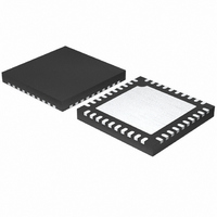
MAX1359BETL+ Maxim Integrated Products, MAX1359BETL+ Datasheet - Page 45

MAX1359BETL+
Manufacturer Part Number
MAX1359BETL+
Description
IC DAS 16BIT 40-TQFN
Manufacturer
Maxim Integrated Products
Type
Data Acquisition System (DAS)r
Specifications of MAX1359BETL+
Resolution (bits)
16 b
Sampling Rate (per Second)
21.84k
Data Interface
Serial
Voltage Supply Source
Analog and Digital
Voltage - Supply
1.8 V ~ 3.6 V
Operating Temperature
-40°C ~ 85°C
Mounting Type
Surface Mount
Package / Case
40-TQFN Exposed Pad
Number Of Converters
2
Resolution
16 bit
Interface Type
Serial (4-Wire, SPI, QSPI, Microwire)
Voltage Reference
1.25 V
Supply Voltage (max)
3.6 V
Supply Voltage (min)
1.8 V
Maximum Power Dissipation
2051.3 mW
Maximum Operating Temperature
+ 85 C
Mounting Style
SMD/SMT
Input Voltage
1.8 V to 3.6 V
Minimum Operating Temperature
- 40 C
Lead Free Status / RoHS Status
Lead free / RoHS Compliant
HFCE: High-frequency-clock enable bit. Set HFCE = 1
to enable the internal high-frequency clock source, and
set HFCE = 0 to disable the high-frequency clock
source.
If HFCE = 1 and CLKE = 1, the internal high-frequency
oscillator is enabled and is present at CLK. The power-
on default state is 1.
CKSEL<2:0>: Clock selection bits. These bits select
the FLL-based output clock frequency at the high-fre-
quency CLK pin as shown in Table 12. The power-on
default state is 001.
IO32E: Input/output 32kHz clock select bit. Set IO32E
= 0 to configure the CLK32K pin as an output, and set
IO32E = 1 to configure the CLK32K pin as an input,
regardless of the signal on the 32KIN pin as shown in
Table 13.
External clock frequencies applied to CLK32K are
clock sources to the FLL, charge pump, and the signal-
detect comparator. The default power-on state is 0.
CK32E: CLK32K output-buffer enable bit. Set CK32E =
1 to enable the CLK32K output buffer as long as OSCE
= 1 and IO32E = 0; otherwise, the CK32E bit is not
asserted. Set CK32E = 0 to disable the CLK32K output
buffer. The power-on default state is 1.
CLKE: CLK output-buffer enable bit. Set CLKE = 1 to
enable the CLK output buffer. Set CLKE = 0 to disable
the buffer. Disabling the buffer is useful for saving
16-Bit, Data-Acquisition System with ADC, DACs,
Table 13. Configuring the CLK32K as an Input or Output
UPIOs, RTC, Voltage Monitors, and Temp Sensor
CLK32K
Output
Input
CLK32K
1
0
______________________________________________________________________________________
IO32E
0
1
32KIN, 32KOUT
XTAL attached
XTAL attached
CLOCK SOURCE
RTC, PWM, WDT
XTAL
XTAL
power in cases where the high-frequency clock is used
internally but is not needed externally. If HFCE = 0, or if
CLKE = 0, CLK remains low. The power-on default
state is 1.
INTP: Interrupt pin polarity bit. Set INTP = 1 to make
INT an active-high output when asserted, and set INTP
= 0 to make INT an active-low output when asserted.
The power-on default state is 1.
WDE: Watchdog-enable bit. Set WDE = 1 to enable the
watchdog timer, which asserts RESET low within 500ms
if the WATCHDOG register is not written. Set WDE = 0
to disable the watchdog timer. The power-on default
state is 0.
Table 12. Setting the CLK Frequency
CLOCK FREQUENCY
4915.2
2457.6
1228.8
32.768
16.384
(kHz)
614.4
8.192
4.096
FLL, C/P, SDC INPUT
SOURCE
CLK32K
XTAL
CKSEL2
0
0
0
0
1
1
1
1
ADC CLOCK SOURCE
CKSEL1
0
0
1
1
0
0
1
1
FLL/HFCLK
FLL/HFCLK
CKSEL0
0
1
0
1
0
1
0
1
45


