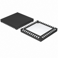
MAX1359BETL+ Maxim Integrated Products, MAX1359BETL+ Datasheet - Page 29

MAX1359BETL+
Manufacturer Part Number
MAX1359BETL+
Description
IC DAS 16BIT 40-TQFN
Manufacturer
Maxim Integrated Products
Type
Data Acquisition System (DAS)r
Specifications of MAX1359BETL+
Resolution (bits)
16 b
Sampling Rate (per Second)
21.84k
Data Interface
Serial
Voltage Supply Source
Analog and Digital
Voltage - Supply
1.8 V ~ 3.6 V
Operating Temperature
-40°C ~ 85°C
Mounting Type
Surface Mount
Package / Case
40-TQFN Exposed Pad
Number Of Converters
2
Resolution
16 bit
Interface Type
Serial (4-Wire, SPI, QSPI, Microwire)
Voltage Reference
1.25 V
Supply Voltage (max)
3.6 V
Supply Voltage (min)
1.8 V
Maximum Power Dissipation
2051.3 mW
Maximum Operating Temperature
+ 85 C
Mounting Style
SMD/SMT
Input Voltage
1.8 V to 3.6 V
Minimum Operating Temperature
- 40 C
Lead Free Status / RoHS Status
Lead free / RoHS Compliant
16-Bit, Data-Acquisition System with ADC, DACs,
Figure 5. Linear-Regulator Block Diagram
The MAX1358B provides voltage supervisors to monitor
DV
DV
sponding LDVD status bit when DV
1.8V threshold voltage. When the DV
rises above the threshold during power-up, RESET
deasserts after a nominal 1.5s timeout period to give the
crystal oscillator time to stabilize. Set the threshold hys-
teresis using the HYSE bit of the PS_VMONS register.
See the PS_VMONS Register section for configuring hys-
teresis. There is no separate voltage monitor for AV
but the analog supply is covered by the DV
many applications where DV
connected together. Multiple supply applications where
AV
separate external voltage monitor for AV
for a block diagram of the DV
The second voltage monitor tracks the charge-pump
output voltage, CPOUT. If CPOUT falls below the 2.7V
threshold, a corresponding register status bit (LCPD) is
DV
UPIOs, RTC, Voltage Monitors, and Temp Sensor
DD
DD
DD
DD
supply voltage. RESET asserts and sets the corre-
and DV
and CPOUT. The first supervisor monitors the
LINEAR 1.65V VOLTAGE REGULATOR
LDOE
1.22V
DD
are not connected together require a
______________________________________________________________________________________
OP
LDOE
DD
DD
Voltage Supervisors
voltage supervisor.
and AV
DD
DD
1.65V
DD
DD
falls below the
supply voltage
. See Figure 7
are externally
DD
monitor in
REG
DD
,
set to flag the condition. The CPOUT monitor output
can also be mapped to the interrupt generator and out-
put on INT. The CPOUT monitor can be used as a 3V
AV
disabled and CPOUT is connected to AV
must be greater or equal to DV
to monitor AV
CPOUT voltage supervisor.
The interrupt generator provides an interrupt to an
external µC. The source of the interrupt is generated by
the status register and can be masked and unmasked
through the IMSK register. CRDY is unmasked by
default, and INT is active-high at power-on reset. INT is
programmable as active-high and active-low. Possible
sources include a rising or falling edge of UPIO_, an
RTC alarm, an ADC conversion completion, or the volt-
age-supervisor outputs. The interrupt causes INT to
assert when configured as an interrupt output.
Figure 6. Charge-Pump Block Diagram
REG
DD
monitor in applications where the charge pump is
M32K
DD.
CLOCK GENERATOR
See Figure 8 for a block diagram of the
NONOVERLAP
CPE
Interrupt Generator (INT)
CHARGE-PUMP DOUBLER
DD
when CPOUT is used
DD
CPOUT
CF-
CF+
. AV
DD
29


