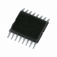
PCA9691TS/1,118 NXP Semiconductors, PCA9691TS/1,118 Datasheet - Page 15

PCA9691TS/1,118
Manufacturer Part Number
PCA9691TS/1,118
Description
IC ADC/DAC 8-BIT I2C 16-TSSOP
Manufacturer
NXP Semiconductors
Type
ADC, DACr
Datasheet
1.PCA9691BS1118.pdf
(31 pages)
Specifications of PCA9691TS/1,118
Package / Case
16-TSSOP
Resolution (bits)
8 b
Data Interface
I²C, Serial
Voltage Supply Source
Single Supply
Voltage - Supply
2.5 V ~ 5.5 V
Operating Temperature
-40°C ~ 85°C
Mounting Type
Surface Mount
Mounting Style
SMD/SMT
Lead Free Status / RoHS Status
Lead free / RoHS Compliant
Sampling Rate (per Second)
-
Lead Free Status / Rohs Status
Lead free / RoHS Compliant
Other names
935283384118
PCA9691TS/1-T
PCA9691TS/1-T
PCA9691TS/1-T
PCA9691TS/1-T
Available stocks
Company
Part Number
Manufacturer
Quantity
Price
Company:
Part Number:
PCA9691TS/1,118
Manufacturer:
NXP
Quantity:
560
NXP Semiconductors
PCA9691_2
Product data sheet
Fig 16. System configuration
SDA
SCL
7.7.3 System configuration
7.7.4 Acknowledge
TRANSMITTER
RECEIVER
MASTER
A device which sends data to the bus is a transmitter, a device which receives data from
the bus is a receiver. The device which initiates and terminates a transfer is the master;
and the devices which are addressed by the master are the slaves (see
The number of data bytes transferred between the START and STOP conditions from
transmitter to receiver is unlimited. Each byte of eight bits is followed by an acknowledge
cycle.
Acknowledgement on the I
Fig 17. Acknowledgement on the I
•
•
•
•
A slave receiver, which is addressed, must generate an acknowledge after the
reception of each byte.
A master receiver must generate an acknowledge after the reception of each byte that
has been clocked out of the slave transmitter.
The device that acknowledges must pull-down the SDA line during the acknowledge
clock pulse, so that the SDA line is stable LOW during the HIGH period of the
acknowledge related clock pulse (set-up and hold times must be taken into
consideration).
A master receiver must signal an end of data to the transmitter by not generating an
acknowledge on the last byte that has been clocked out of the slave. In this event, the
transmitter must leave the data line HIGH to enable the master to generate a STOP
condition.
by transmitter
data output
data output
by receiver
SCL from
master
RECEIVER
SLAVE
condition
START
Rev. 02 — 27 January 2010
S
2
C-bus is illustrated in
TRANSMITTER
RECEIVER
SLAVE
1
2
C-bus
2
TRANSMITTER
Figure
MASTER
17.
not acknowledge
8-bit A/D and D/A converter
acknowledge
8
TRANSMITTER
RECEIVER
MASTER
acknowledgement
clock pulse for
PCA9691
© NXP B.V. 2010. All rights reserved.
Figure
mba605
9
mbc602
16).
15 of 31


