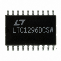
LTC1296DCSW Linear Technology, LTC1296DCSW Datasheet - Page 20

LTC1296DCSW
Manufacturer Part Number
LTC1296DCSW
Description
IC DATA ACQ SYSTEM 12BIT 20-SOIC
Manufacturer
Linear Technology
Type
Data Acquisition System (DAS), ADCr
Datasheet
1.LTC1296CCSWPBF.pdf
(28 pages)
Specifications of LTC1296DCSW
Resolution (bits)
12 b
Sampling Rate (per Second)
46.5k
Data Interface
Serial, Parallel
Voltage Supply Source
Dual ±
Voltage - Supply
±5V
Operating Temperature
0°C ~ 70°C
Mounting Type
Surface Mount
Package / Case
20-SOIC (7.5mm Width)
Lead Free Status / RoHS Status
Contains lead / RoHS non-compliant
Other names
LTC1296DCS
Available stocks
Company
Part Number
Manufacturer
Quantity
Price
Part Number:
LTC1296DCSW
Manufacturer:
LINEAR/凌特
Quantity:
20 000
Company:
Part Number:
LTC1296DCSW#PBF
Manufacturer:
LT
Quantity:
2 122
within the minimum settling windows of 2.5µs (“+” input)
and 1µs(“–” input) that occurs at the maximum clock rate
of 1MHz. Figures 9 and 10 show examples of adequate
and poor op amp settling.
LTC1293/LTC1294/LTC1296
A
RC Input Filtering
It is possible to filter the inputs with an RC network as
shown in Figure 11. For large values of C
capacitive input switching currents are averaged into a net
DC current. A filter should be chosen with a small resistor
and large capacitor to prevent DC drops across the resis-
tor. The magnitude of the DC current is approximately I
= 100pF × V
When running at the minimum cycle time of 21.5µs, the
input current equals 23µA at V
of 5Ω will cause 0.1LSB of full-scale error. If a larger filter
resistor must be used, errors can be reduced by increasing
20
Figure 9. Adequate Settling of Op Amp Driving Analog Input
PPLICATI
Figure 10. Poor Op Amp Settling Can Cause A/D Errors
V
IN
IN
/t
–
Figure 11. RC Input Filtering
CYC
O
R
FILTER
U
and is roughly proportional to V
HORIZONTAL: 500ns/DIV
HORIZONTAL: 20µs/DIV
S
I
IDC
I FOR ATIO
U
C
FILTER
IN
= 5V. Here a filter resistor
"+"
"–"
LTC1293/4/6
W
LTC1293 F11
F
(e.g., 1µF) the
U
DC
IN
.
the cycle time as shown in the typical performance char-
acteristic curve Maximum Filter Resistor vs Cycle Time.
Input Leakage Current
Input leakage currents also can create errors if the source
resistance gets too large. For example, the maximum input
leakage specification of 1µA (at 125°C) flowing through a
source resistance of 1kΩ will cause a voltage drop of 1mV
or 0.8LSB. This error will be much reduced at lower
temperatures because leakage drops rapidly (see typical
performance characteristic curve Input Channel Leakage
Current vs Temperature).
SAMPLE AND HOLD
Single-Ended Input
The LTC1293/4/6 provides a built-in sample and hold
(S&H) function for all signals acquired in the single-ended
mode (COM pin grounded). The sample and hold allows
the LTC1293/4/6 to convert rapidly varying signals (see
typical performance characteristic curve of S&H Acquisi-
tion Time vs Source Resistance). The input voltage is
sampled during the t
sampling interval begins as the bit preceding the MSBF bit
is shifted in and continues until the falling edge of the PS
bit is received. On this falling edge the S&H goes into the
hold mode and the conversion begins.
Differential Input
With a differential input the A/D no longer converts a
single voltage but converts the difference between two
voltages. The voltage on the selected “+” input is sampled
and held and can be rapidly time varying. The voltage on
the “–” pin must remain constant and be free of noise and
ripple throughout the conversion time. Otherwise the
differencing operation will not be done accurately. The
conversion time is 12 CLK cycles. Therefore a change in
the –IN input voltage during this interval can cause con-
version errors. For a sinusoidal voltage on the –IN input
this error would be:
Where f
is its peak amplitude and f
V
ERROR MAX
(–)
is the frequency of the “–” input voltage, V
(
)
=
(
2
SMPL
π
f V
(–)
CLK
time as shown in Figure 8. The
PEAK
is the frequency of the CLK.
)
⎛
⎜
⎝
f
CLK
12
⎞
⎟
⎠
129346fs
PEAK


