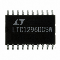
LTC1296DCSW Linear Technology, LTC1296DCSW Datasheet - Page 10

LTC1296DCSW
Manufacturer Part Number
LTC1296DCSW
Description
IC DATA ACQ SYSTEM 12BIT 20-SOIC
Manufacturer
Linear Technology
Type
Data Acquisition System (DAS), ADCr
Datasheet
1.LTC1296CCSWPBF.pdf
(28 pages)
Specifications of LTC1296DCSW
Resolution (bits)
12 b
Sampling Rate (per Second)
46.5k
Data Interface
Serial, Parallel
Voltage Supply Source
Dual ±
Voltage - Supply
±5V
Operating Temperature
0°C ~ 70°C
Mounting Type
Surface Mount
Package / Case
20-SOIC (7.5mm Width)
Lead Free Status / RoHS Status
Contains lead / RoHS non-compliant
Other names
LTC1296DCS
Available stocks
Company
Part Number
Manufacturer
Quantity
Price
Part Number:
LTC1296DCSW
Manufacturer:
LINEAR/凌特
Quantity:
20 000
Company:
Part Number:
LTC1296DCSW#PBF
Manufacturer:
LT
Quantity:
2 122
LTC1293/LTC1294/LTC1296
the half duplex operation D
together allowing transmission over just 3 wired: CS, CLK
and DATA (D
chip select (CS) signal. After CS falls the LTC1293/4/6
looks for a start bit. After the start bit is received a 7-bit
input word is shifted into the D
the LTC1293/4/6 and starts the conversion. After one null
bit, the result of the conversion is output on the D
With the half duplex serial interface the D
the current conversion. After the end of the data exchange
CS should be brought high. This resets the LTC1293/4/6
in preparation for the next data exchange.
10
A
The LTC 1293/4/6 is a data acquisition component which
contains the following functional blocks:
1. 12-bit successive approximation capacitive A/D
2. Analog multiplexer (MUX)
3. Sample and hold (S/H)
4. Synchronous, half duplex serial interface
5. Control and timing logic
DIGITAL CONSIDERATIONS
Serial Interface
The LTC1293/4/6 communicates with microprocessors
and other external circuitry via a synchronous, half duplex,
four-wire serial interface (see Operating Sequence). The
clock (CLK) synchronizes the data transfer with each bit
being transmitted on the falling CLK edge and captured on
the rising CLK edge in both transmitting and receiving
systems. The input data is first received and then the A/D
conversion result is transmitted (half duplex). Because of
PPLICATI
converter
CS
SHIFT MUX
ADDRESS IN
IN
/D
D
IN
OUT
O
1
U
). Data transfer is initiated by a falling
1 NULL
BIT
S
I FOR ATIO
U
SHIFT A/D CONVERSION
RESULT OUT
IN
IN
and D
input which configures
W
D
OUT
OUT
OUT
1
may be tied
data is from
U
OUT
line.
D
IN
Start Bit
The first "logical one" clocked into the D
goes low is the start bit. The start bit initiates the data
transfer and all leading zeroes which precede this logical
one will be ignored. After the start bit is received the
remaining bits of the input word will be clocked in. Further
inputs on the D
cycle.
MUX Address
The four bits of the input word following the START BIT
assign the MUX configuration for the requested conver-
sion. For a given channel selection, the converter will
measure the voltage between the two channels indicated
by the + and – signs in the selected row of the following
table. Note that in differential mode (SGL/DIFF = 0) mea-
surements are limited to four adjacent input pairs with
either polarity. In single ended mode, all input channels
are measured with respect to COM. Only the +inputs have
sample and holds. Signals applied at the –inputs must not
change more than the required accuracy during the con-
version.
INPUT DATA WORD
The LTC1293/4/6 seven-bit data word is clocked into the
D
goes low and the start bit has been recognized. Further
inputs on the D
cycle. The input word is defined as follows:
2
START
IN
input on the rising edge of the clock after chip select
SGL/
DIFF
IN
ODD/
SIGN
IN
MUX ADDRESS
pin are then ignored until the next CS
pin are then ignored until the next CS
SELECT
D
OUT
1
2
SELECT
0
UNIPOLAR/
BIPOLAR
UNI
IN
MSB FIRST/
input after CS
LSB FIRST
MSBF
LTC1293 AI01
SHUTDOWN
POWER
129346fs
LTC1293 AI02
PS


