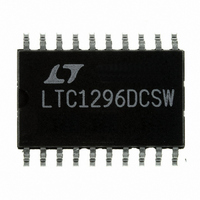
LTC1296DCSW Linear Technology, LTC1296DCSW Datasheet - Page 17

LTC1296DCSW
Manufacturer Part Number
LTC1296DCSW
Description
IC DATA ACQ SYSTEM 12BIT 20-SOIC
Manufacturer
Linear Technology
Type
Data Acquisition System (DAS), ADCr
Datasheet
1.LTC1296CCSWPBF.pdf
(28 pages)
Specifications of LTC1296DCSW
Resolution (bits)
12 b
Sampling Rate (per Second)
46.5k
Data Interface
Serial, Parallel
Voltage Supply Source
Dual ±
Voltage - Supply
±5V
Operating Temperature
0°C ~ 70°C
Mounting Type
Surface Mount
Package / Case
20-SOIC (7.5mm Width)
Lead Free Status / RoHS Status
Contains lead / RoHS non-compliant
Other names
LTC1296DCS
Available stocks
Company
Part Number
Manufacturer
Quantity
Price
Part Number:
LTC1296DCSW
Manufacturer:
LINEAR/凌特
Quantity:
20 000
Company:
Part Number:
LTC1296DCSW#PBF
Manufacturer:
LT
Quantity:
2 122
A
Sharing the Serial Interface
The LTC1293/4/6 can share the same 3-wire serial inter-
face with other peripheral components or other LTC1293/
4/6’s (Figure 3). Now, the CS signals decide which LTC1293/
4/6 is being addressed by the MPU.
ANALOG CONSIDERATIONS
Grounding
The LTC1293/4/6 should be used with an analog ground
plane and single point grounding techniques. Do not use
wire wrapping techniques to breadboard and evaluate the
8051 CODE
LABEL MNEMONIC
CONT
LOOP1 RLC
LOOP
PPLICATI
SETB
MOV
CLR
MOV
CLR
MOV
SETB
DJNZ
MOV
CLR
MOV
MOV
RLC
SETB
CLR
DJNZ
MOV
MOV
SETB
O
OPERAND
P1.4
A,#87H
P1.4
R4,#08H
A
P1.3
P1.2,C
P1.3
R4,LOOP1
P1,#04H
P1.3
R4,#09H
C,P1.2
A
P1.3
P1.3
R4,LOOP
R2,A
C,P1.2
P1.3
U
S
I FOR ATIO
U
COMMENTS
CS GOES HIGH
DIN WORD FOR LTC1294
CS GOES LOW
LOAD COUNTER
ROTATE DIN BIT INTO CARRY
CLK GOES LOW
OUTPUT DIN BIT TO LTC1294
CLK GOES HIGH
NEXT DIN BIT
P1.2 BECOMES AN INPUT
CLK GOES LOW
LOAD COUNTER
READ DATA BIT INTO CARRY
ROTATE DATA BIT (B3) INTO ACC
CLK GOES HIGH
CLK GOES LOW
NEXT DOUT BIT
STORE MSBs IN R2
READ DATA BIT INTO CARRY
CLK GOES HIGH
Figure 3. Several LTC1294 Sharing One 3-Wire Serial Interface
OUTPUT PORT
W
2
SERIAL DATA
1
MPU
0
U
3
3
8 CHANNELS
LTC1294
CS
LABEL MNEMONIC
device. To achieve the optimum performance use a PC
board. The analog ground pin (AGND) should be tied
directly to the ground plane with minimum lead length (a
low profile socket is fine). The digital ground pin (DGND)
also can be tied directly to this ground pin because
minimal digital noise is generated within the chip itself.
V
(minimum value) tantalum with leads as short as possible
and as close as possible to the pin. A 0.1µF ceramic disk
also should be placed in parallel with the 22µF and again
with leads as short as possible and as close to V
possible. AV
3
CC
8 CHANNELS
LTC1294
should be bypassed to the ground plane with a 22µF
CLR
CLR
RLC
MOV
RLC
SETB
CLR
MOV
RLC
SETB
CLR
MOV
SETB
RRC
RRC
RRC
RRC
MOV
AJMP
CS
LTC1293/LTC1294/LTC1296
CC
3
8 CHANNELS
LTC1294
and DV
OPERAND
P1.3
A
A
C,P1.2
A
P1.3
P1.3
C,P1.2
A
P1.3
P1.3
C,P1.2
P1.4
A
A
A
A
R3,A
CONT
CS
CC
3-WIRE SERIAL
INTERFACE TO OTHER
PERIPHERALS OR LTC1293/4/6s
should be tied together on the
COMMENTS
CLK GOES LOW
CLEAR ACC
ROTATE DATA BIT (B3) INTO ACC
READ DATA BIT INTO CARRY
ROTATE DATA BIT (B2) INTO ACC
CLK GOES HIGH
CLK GOES LOW
READ DATA BIT INTO CARRY
ROTATE DATA BIT (B1) INTO ACC
CLK GOES HIGH
CLK GOES LOW
READ DATA BIT INTO CARRY
CS GOES HIGH
ROTATE DATA BIT (B0) INTO ACC
ROTATE RIGHT INTO ACC
ROTATE RIGHT INTO ACC
ROTATE RIGHT INTO ACC
STORE LSBs IN R3
START NEXT CONVERSION
LTC1293 F03
17
129346fs
CC
as


