PCF8591P,112 NXP Semiconductors, PCF8591P,112 Datasheet - Page 4
PCF8591P,112
Manufacturer Part Number
PCF8591P,112
Description
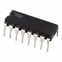
IC ADC/DAC 8-BIT I2C 16-DIP
Manufacturer
NXP Semiconductors
Type
ADC, DACr
Datasheet
1.PCF8591T2518.pdf
(28 pages)
Specifications of PCF8591P,112
Package / Case
16-DIP (0.300", 7.62mm)
Resolution (bits)
8 b
Sampling Rate (per Second)
11.1k
Data Interface
I²C, Serial
Voltage Supply Source
Dual ±
Voltage - Supply
2.5 V ~ 6 V
Operating Temperature
-40°C ~ 85°C
Mounting Type
Through Hole
Resolution
8 bit
Interface Type
I2C
Supply Voltage (max)
6 V
Supply Voltage (min)
2.5 V
Mounting Style
Through Hole
Lead Free Status / RoHS Status
Lead free / RoHS Compliant
Lead Free Status / RoHS Status
Lead free / RoHS Compliant, Lead free / RoHS Compliant
Other names
568-1087-5
933768130112
PCF8591PN
933768130112
PCF8591PN


Philips Semiconductors
5
6
2003 Jan 27
handbook, full pagewidth
AINO
AIN1
AIN2
AIN3
A0
A1
A2
V
SDA
SCL
OSC
EXT
AGND
V
AOUT
V
SS
REF
DD
8-bit A/D and D/A converter
SYMBOL
BLOCK DIAGRAM
PINNING
PIN
10
11
12
13
14
15
16
AOUT
1
2
3
4
5
6
7
8
9
AIN0
AIN1
AIN2
AIN3
OSC
V DD
SDA
V SS
SCL
EXT
A0
A1
A2
negative supply voltage
I
I
oscillator input/output
external/internal switch for
oscillator input
analog ground
voltage reference input
analog output (D/A converter)
positive supply voltage
analog inputs (A/D converter)
hardware address
2
2
C-bus data input/output
C-bus clock input
MULTIPLEXER
POWER ON
INTERFACE
ANALOGUE
I
RESET
2
C BUS
DESCRIPTION
OSCILLATOR
SAMPLE
SAMPLE
PCF8591
HOLD
HOLD
AND
AND
Fig.1 Block diagram.
4
COMPARATOR
handbook, halfpage
REGISTER
CONTROL
STATUS
LOGIC
Fig.2 Pinning diagram (DIP16).
REGISTER
DAC DATA
AIN0
AIN1
AIN2
AIN3
V SS
A0
A1
A2
REGISTER/LOGIC
APPROXIMATION
SUCCESSIVE
1
2
3
4
5
6
7
8
PCF8591P
DAC
REGISTER
ADC DATA
MBL822
MBL821
16
15
14
13
12
11
10
9
Product specification
V DD
AOUT
V REF
AGND
EXT
OSC
SCL
SDA
PCF8591
V REF
AGND
Related parts for PCF8591P,112
Image
Part Number
Description
Manufacturer
Datasheet
Request
R

Part Number:
Description:
IC, A/D AND D/A CONVERTER, 8BIT, 16-DIP
Manufacturer:
NXP Semiconductors
Datasheet:

Part Number:
Description:
8-bit A/d And D/a Converter
Manufacturer:
NXP Semiconductors
Datasheet:
Part Number:
Description:
NXP Semiconductors designed the LPC2420/2460 microcontroller around a 16-bit/32-bitARM7TDMI-S CPU core with real-time debug interfaces that include both JTAG andembedded trace
Manufacturer:
NXP Semiconductors
Datasheet:

Part Number:
Description:
NXP Semiconductors designed the LPC2458 microcontroller around a 16-bit/32-bitARM7TDMI-S CPU core with real-time debug interfaces that include both JTAG andembedded trace
Manufacturer:
NXP Semiconductors
Datasheet:
Part Number:
Description:
NXP Semiconductors designed the LPC2468 microcontroller around a 16-bit/32-bitARM7TDMI-S CPU core with real-time debug interfaces that include both JTAG andembedded trace
Manufacturer:
NXP Semiconductors
Datasheet:
Part Number:
Description:
NXP Semiconductors designed the LPC2470 microcontroller, powered by theARM7TDMI-S core, to be a highly integrated microcontroller for a wide range ofapplications that require advanced communications and high quality graphic displays
Manufacturer:
NXP Semiconductors
Datasheet:
Part Number:
Description:
NXP Semiconductors designed the LPC2478 microcontroller, powered by theARM7TDMI-S core, to be a highly integrated microcontroller for a wide range ofapplications that require advanced communications and high quality graphic displays
Manufacturer:
NXP Semiconductors
Datasheet:
Part Number:
Description:
The Philips Semiconductors XA (eXtended Architecture) family of 16-bit single-chip microcontrollers is powerful enough to easily handle the requirements of high performance embedded applications, yet inexpensive enough to compete in the market for hi
Manufacturer:
NXP Semiconductors
Datasheet:
Part Number:
Description:
The XA-S3 device is a member of Philips Semiconductors? XA(eXtended Architecture) family of high performance 16-bitsingle-chip microcontrollers
Manufacturer:
NXP Semiconductors
Datasheet:

Part Number:
Description:
The NXP BlueStreak LH75401/LH75411 family consists of two low-cost 16/32-bit System-on-Chip (SoC) devices
Manufacturer:
NXP Semiconductors
Datasheet:
Part Number:
Description:
The NXP LPC3130/3131 combine an 180 MHz ARM926EJ-S CPU core, high-speed USB2
Manufacturer:
NXP Semiconductors
Datasheet:
Part Number:
Description:
The NXP LPC3141 combine a 270 MHz ARM926EJ-S CPU core, High-speed USB 2
Manufacturer:
NXP Semiconductors
Part Number:
Description:
The NXP LPC3143 combine a 270 MHz ARM926EJ-S CPU core, High-speed USB 2
Manufacturer:
NXP Semiconductors

Part Number:
Description:
The NXP LPC3152 combines an 180 MHz ARM926EJ-S CPU core, High-speed USB 2
Manufacturer:
NXP Semiconductors