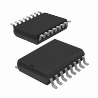
PCF8591T/2,518 NXP Semiconductors, PCF8591T/2,518 Datasheet - Page 9

PCF8591T/2,518
Manufacturer Part Number
PCF8591T/2,518
Description
IC ADC/DAC 8-BIT I2C 16-SOIC
Manufacturer
NXP Semiconductors
Type
ADC, DACr
Datasheet
1.PCF8591T2518.pdf
(28 pages)
Specifications of PCF8591T/2,518
Package / Case
16-SOIC (0.300", 7.5mm Width)
Resolution (bits)
8 b
Sampling Rate (per Second)
11.1k
Data Interface
I²C, Serial
Voltage Supply Source
Dual ±
Voltage - Supply
2.5 V ~ 6 V
Operating Temperature
-40°C ~ 85°C
Mounting Type
Surface Mount
Mounting Style
SMD/SMT
Lead Free Status / RoHS Status
Lead free / RoHS Compliant
Lead Free Status / RoHS Status
Lead free / RoHS Compliant, Lead free / RoHS Compliant
Other names
568-1088-2
935276541518
PCF8591TD-T
935276541518
PCF8591TD-T
Available stocks
Company
Part Number
Manufacturer
Quantity
Price
Part Number:
PCF8591T/2,518
Manufacturer:
NXP/恩智浦
Quantity:
20 000
Philips Semiconductors
7.4
The A/D converter makes use of the successive
approximation conversion technique. The on-chip D/A
converter and a high-gain comparator are used
temporarily during an A/D conversion cycle.
An A/D conversion cycle is always started after sending a
valid read mode address to a PCF8591 device. The A/D
conversion cycle is triggered at the trailing edge of the
acknowledge clock pulse and is executed while
transmitting the result of the previous conversion (see
Fig.9).
Once a conversion cycle is triggered an input voltage
sample of the selected channel is stored on the chip and is
2003 Jan 27
handbook, full pagewidth
8-bit A/D and D/A converter
PROTOCOL
A/D conversion
SDA
SCL
S
1
ADDRESS
2
1
8
A
9
conversion of byte 1
Fig.9 A/D conversion sequence.
sampling byte 1
1
converted byte
DATA BYTE 0
transmission
of previously
9
converted to the corresponding 8-bit binary code. Samples
picked up from differential inputs are converted to an 8-bit
twos complement code (see Figs 10 and 11).
The conversion result is stored in the ADC data register
and awaits transmission. If the auto-increment flag is set
the next channel is selected.
The first byte transmitted in a read cycle contains the
conversion result code of the previous read cycle. After a
Power-on reset condition the first byte read is a
hexadecimal 80. The protocol of an I
shown in Chapter 8, Figs 16 and 17.
The maximum A/D conversion rate is given by the actual
speed of the I
A
9
conversion of byte 2
1
sampling byte 2
DATA BYTE 1
transmission
of byte 1
2
C-bus.
A
9
1
conversion of byte 3
sampling byte 3
DATA BYTE 2
transmission
of byte 2
2
Product specification
C-bus read cycle is
PCF8591
A
MBL829


