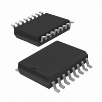
PCF8591T/2,518 NXP Semiconductors, PCF8591T/2,518 Datasheet - Page 13

PCF8591T/2,518
Manufacturer Part Number
PCF8591T/2,518
Description
IC ADC/DAC 8-BIT I2C 16-SOIC
Manufacturer
NXP Semiconductors
Type
ADC, DACr
Datasheet
1.PCF8591T2518.pdf
(28 pages)
Specifications of PCF8591T/2,518
Package / Case
16-SOIC (0.300", 7.5mm Width)
Resolution (bits)
8 b
Sampling Rate (per Second)
11.1k
Data Interface
I²C, Serial
Voltage Supply Source
Dual ±
Voltage - Supply
2.5 V ~ 6 V
Operating Temperature
-40°C ~ 85°C
Mounting Type
Surface Mount
Mounting Style
SMD/SMT
Lead Free Status / RoHS Status
Lead free / RoHS Compliant
Lead Free Status / RoHS Status
Lead free / RoHS Compliant, Lead free / RoHS Compliant
Other names
568-1088-2
935276541518
PCF8591TD-T
935276541518
PCF8591TD-T
Available stocks
Company
Part Number
Manufacturer
Quantity
Price
Part Number:
PCF8591T/2,518
Manufacturer:
NXP/恩智浦
Quantity:
20 000
Philips Semiconductors
8.3
A device generating a message is a ‘transmitter’, a device receiving a message is the ‘receiver’. The device that controls
the message is the ‘master’ and the devices which are controlled by the master are the ‘slaves’.
8.4
The number of data bytes transferred between the start and stop conditions from transmitter to receiver is not limited.
Each data byte of eight bits is followed by one acknowledge bit. The acknowledge bit is a HIGH level put on the bus by
the transmitter whereas the master also generates an extra acknowledge related clock pulse. A slave receiver which is
addressed must generate an acknowledge after the reception of each byte. Also a master must generate an
acknowledge after the reception of each byte that has been clocked out of the slave transmitter. The device that
acknowledges has to pull down the SDA line during the acknowledge clock pulse, so that the SDA line is stable LOW
during the HIGH period of the acknowledge related clock pulse. A master receiver must signal an end of data to the
transmitter by not generating an acknowledge on the last byte that has been clocked out of the slave. In this event the
transmitter must leave the data line HIGH to enable the master to generate a stop condition.
2003 Jan 27
handbook, full pagewidth
8-bit A/D and D/A converter
System configuration
Acknowledge
SDA
SCL
BY TRANSMITTER
TRANSMITTER /
DATA OUTPUT
RECEIVER
DATA OUTPUT
BY RECEIVER
MASTER
SCL FROM
MASTER
condition
START
S
RECEIVER
Fig.15 Acknowledgement on the I
SLAVE
Fig.14 System configuration.
1
TRANSMITTER /
RECEIVER
13
SLAVE
2
2
C-bus.
TRANSMITTER
not acknowledge
MASTER
acknowledge
8
acknowledgement
clock pulse for
9
TRANSMITTER /
RECEIVER
MBC602
MASTER
Product specification
PCF8591
MBA605


